- 您现在的位置:买卖IC网 > PDF目录378277 > ADC081500 (National Semiconductor Corporation) High Performance, Low Power, 8-Bit, 1.5 GSPS A/D Converter PDF资料下载
参数资料
| 型号: | ADC081500 |
| 厂商: | National Semiconductor Corporation |
| 英文描述: | High Performance, Low Power, 8-Bit, 1.5 GSPS A/D Converter |
| 中文描述: | 高性能,低功耗,8位,1.5 GSPS的A / D转换 |
| 文件页数: | 25/28页 |
| 文件大小: | 830K |
| 代理商: | ADC081500 |
第1页第2页第3页第4页第5页第6页第7页第8页第9页第10页第11页第12页第13页第14页第15页第16页第17页第18页第19页第20页第21页第22页第23页第24页当前第25页第26页第27页第28页
2.0 Applications Information
(Continued)
sequence is complete. However, if power is applied and PD
is already high, the device will not begin the calibration
sequence until the PD input goes low. If a manual calibration
is requested while the device is powered down, the calibra-
tion will not begin at all. That is, the manual calibration input
is completely ignored in the power down state.
2.5 THE DIGITAL OUTPUTS
The ADC081500 demultiplexes the converter output data
into two LVDS output buses. The results of successive con-
versions started on the odd falling edges of the CLK+ pin are
available on one of the two LVDS buses, while the results of
conversions started on the even falling edges of the CLK+
pin are available on the other LVDS bus. This means that,
the word rate at each LVDS bus is 1/2 the ADC081500 input
clock rate and the two buses must be multiplexed to obtain
the entire 1.5 GSPS conversion result.
Since the minimum recommended input clock rate for this
device is 200 MHz, the effective data rate can be reduced to
as low as 100 MSPS by using the results available on just
one of the output buses with a 200 MHz input clock, deci-
mating the 200 MSPS data by two.
There is one LVDS output clock pair (DCLK+/-) available for
use to latch the LVDS outputs on all buses. Whether the data
is sent at the rising or falling edge of DCLK is determined by
the sense of the OutEdge pin, as described in Section 2.4.3.
DDR (Double Data Rate) clocking can also be used. In this
mode a word of data is presented with each edge of DCLK,
reducing the DCLK frequency to 1/4 the input clock fre-
quency. See the Timing Diagram section for details.
The OutV pin is used to set the LVDS differential output
levels. See Section 2.4.4.
The output format is Offset Binary. Accordingly, a full-scale
input level with V
+ positive with respect to V
will pro-
duce an output code of all ones, a full-scale input level with
V
positive with respect to V
IN
+ will produce an output
code of all zeros and when V
+ and V
are equal, the
output code will vary between codes 127 and 128.
2.6 POWER CONSIDERATIONS
A/D converters draw sufficient transient current to corrupt
their own power supplies if not adequately bypassed. A 33
μF capacitor should be placed within an inch (2.5 cm) of the
A/D converter power pins. A 0.1 μF capacitor should be
placed as close as possible to each V
A
pin, preferably within
one-half centimeter. Leadless chip capacitors are preferred
because they have low lead inductance.
The V
and V
supply pins should be isolated from each
other to prevent any digital noise from being coupled into the
analog portions of the ADC. A ferrite choke, such as the JW
Miller FB20009-3B, is recommended between these supply
lines when a common source is used for them.
As is the case with all high speed converters, the
ADC081500 should be assumed to have little power supply
noise rejection. Any power supply used for digital circuitry in
a system where a lot of digital power is being consumed
should not be used to supply power to the ADC081500. The
ADC supplies should be the same supply used for other
analog circuitry, if not a dedicated supply.
2.6.1 Supply Voltage
TheADC081500 is specified to operate with a supply voltage
of 1.9V
±
0.1V. It is very important to note that, while this
device will function with slightly higher supply voltages,
these higher supply voltages may reduce product lifetime.
No pin should ever have a voltage on it that is in excess of
the supply voltage or below ground by more than 150 mV,
not even on a transient basis. This can be a problem upon
application of power and power shut-down. Be sure that the
supplies to circuits driving any of the input pins, analog or
digital, do not come up any faster than does the voltage at
the ADC081500 power pins.
The Absolute Maximum Ratings should be strictly observed,
even during power up and power down. A power supply that
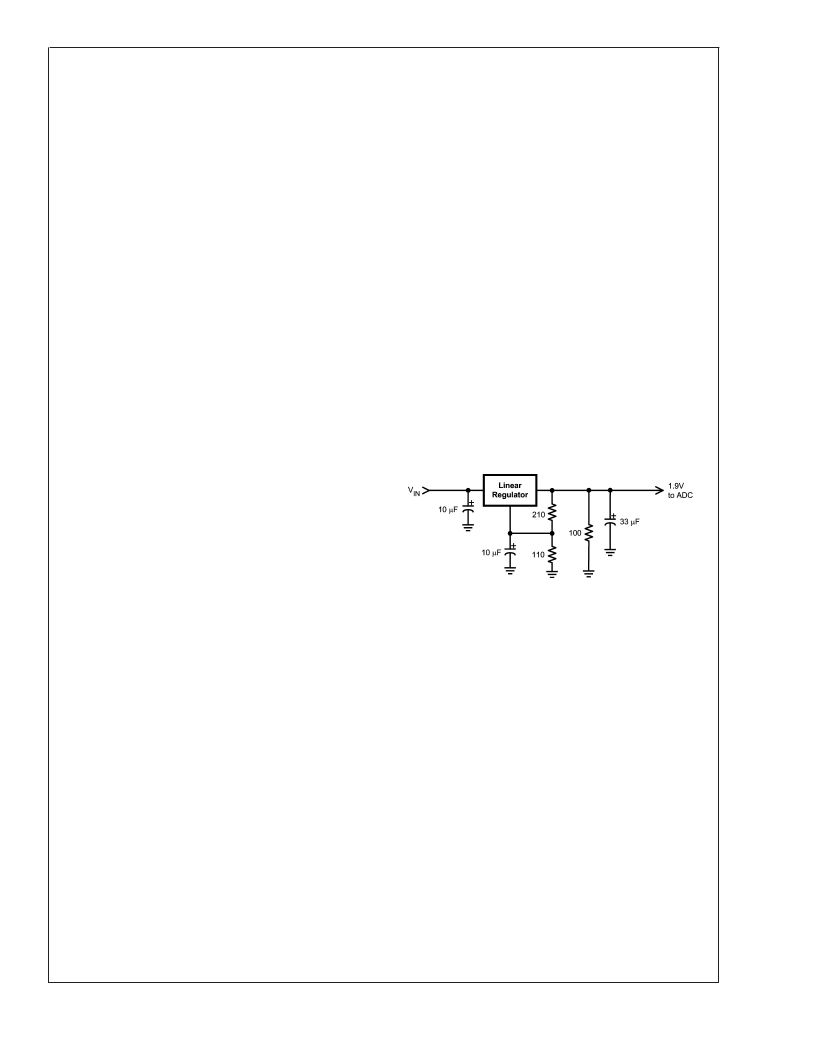
produces a voltage spike at turn-on and/or turn-off of power
can destroy the ADC081500. The circuit of
Figure 15
will
provide supply overshoot protection.
Many linear regulators will produce output spiking at
power-on unless there is a minimum load provided. Active
devices draw very little current until their supply voltages
reach a few hundred millivolts. The result can be a turn-on
spike that can destroy the ADC081500, unless a minimum
load is provided for the supply. The 100
resistor at the
regulator output provides a minimum output current during
power-up to ensure there is no turn-on spiking.
In the circuit of
Figure 15
, an LM317 linear regulator is
satisfactory if its input supply voltage is 4V to 5V . If a 3.3V
supply is used, an LM1086 linear regulator is recommended.
The output drivers should have a supply voltage, V
, that is
within the range specified in the Operating Ratings table.
This voltage should not exceed the V
A
supply voltage.
If the power is applied to the device without an input clock
signal present, the current drawn by the device might be
below 200 mA. This is because the ADC081500 gets reset
through clocked logic and its initial state is unknown. If the
reset logic comes up in the "on" state, it will cause most of
the analog circuitry to be powered down, resulting in less
than 100 mA of current draw. This current is greater than the
power down current because not all of the ADC is powered
down. The device current will be normal after the input clock
is established.
2.6.2 Thermal Management
The ADC081500 is capable of impressive speeds and per-
formance at very low power levels for its speed. However,
the power consumption is still high enough to require atten-
tion to thermal management. For reliability reasons, the die
temperature should be kept to a maximum of 130C. That is,
T
(ambient temperature) plus ADC power consumption
times
θ
JA
(junction to ambient thermal resistance) should not
20153154
FIGURE 15. Non-Spiking Power Supply
A
www.national.com
25
相关PDF资料 |
PDF描述 |
|---|---|
| ADC081500CIYB | High Performance, Low Power, 8-Bit, 1.5 GSPS A/D Converter |
| ADC081500EVAL | High Performance, Low Power, 8-Bit, 1.5 GSPS A/D Converter |
| ADC08161 | 500 ns A/D Converter with S/H Function and 2.5V Bandgap Reference(500ns带S/H功能和2.5V带隙参考的A/D转换器) |
| ADC08161CIWM | 500 ns A/D Converter with S/H Function and 2.5V Bandgap Reference |
| ADC0816 | 8-BitμP Compatible A/D Converters with 16-Channel Multiplexer(带16通道多路器的8位μP兼容A/D转换器) |
相关代理商/技术参数 |
参数描述 |
|---|---|
| ADC081500_06 | 制造商:NSC 制造商全称:National Semiconductor 功能描述:High Performance, Low Power, 8-Bit, 1.5 GSPS A/D Converter |
| ADC081500_09 | 制造商:NSC 制造商全称:National Semiconductor 功能描述:High Performance, Low Power, 8-Bit, 1.5 GSPS A/D Converter |
| ADC081500CIYB | 功能描述:模数转换器 - ADC RoHS:否 制造商:Texas Instruments 通道数量:2 结构:Sigma-Delta 转换速率:125 SPs to 8 KSPs 分辨率:24 bit 输入类型:Differential 信噪比:107 dB 接口类型:SPI 工作电源电压:1.7 V to 3.6 V, 2.7 V to 5.25 V 最大工作温度:+ 85 C 安装风格:SMD/SMT 封装 / 箱体:VQFN-32 |
| ADC081500CIYB/NOPB | 功能描述:模数转换器 - ADC RoHS:否 制造商:Texas Instruments 通道数量:2 结构:Sigma-Delta 转换速率:125 SPs to 8 KSPs 分辨率:24 bit 输入类型:Differential 信噪比:107 dB 接口类型:SPI 工作电源电压:1.7 V to 3.6 V, 2.7 V to 5.25 V 最大工作温度:+ 85 C 安装风格:SMD/SMT 封装 / 箱体:VQFN-32 |
| ADC081500DEV | 制造商:NSC 制造商全称:National Semiconductor 功能描述:High Performance, Low Power, 8-Bit, 1.5 GSPS A/D Converter |
发布紧急采购,3分钟左右您将得到回复。