- 您现在的位置:买卖IC网 > PDF目录378277 > ADC081500 (National Semiconductor Corporation) High Performance, Low Power, 8-Bit, 1.5 GSPS A/D Converter PDF资料下载
参数资料
| 型号: | ADC081500 |
| 厂商: | National Semiconductor Corporation |
| 英文描述: | High Performance, Low Power, 8-Bit, 1.5 GSPS A/D Converter |
| 中文描述: | 高性能,低功耗,8位,1.5 GSPS的A / D转换 |
| 文件页数: | 22/28页 |
| 文件大小: | 830K |
| 代理商: | ADC081500 |
第1页第2页第3页第4页第5页第6页第7页第8页第9页第10页第11页第12页第13页第14页第15页第16页第17页第18页第19页第20页第21页当前第22页第23页第24页第25页第26页第27页第28页
2.0 Applications Information
(Continued)
and 840 mV
in the Extended Control mode through the
Serial Interface. For best performance, it is recommended
that the full-scale range be kept between 595 mV
P-P
and 805
mV
P-P
.
Table 4
gives the input to output relationship with the FSR
pin high and the normal (non-extended) mode is used. With
the FSR pin grounded, the millivolt values in
Table 4
are
reduced to 75% of the values indicated. In the Enhanced
Control Mode, these values will be determined by the full
scale range and offset settings in the Control Registers.
TABLE 4. DIFFERENTIAL INPUT TO OUTPUT
RELATIONSHIP (Normal Control Mode, FSR High)
V
IN
+
V
IN
Output Code
0000 0000
0100 0000
0111 1111 /
1000 0000
1100 0000
1111 1111
V
CM
217.5mV
V
CM
109 mV
V
CM
+ 217.5mV
V
CM
+ 109 mV
V
CM
V
CM
V
CM
+ 109 mV
V
CM
+ 217.5mV
V
CM
109 mV
V
CM
217.5mV
The buffered analog inputs simplify the task of driving these
inputs and the RC pole that is generally used at sampling
ADC inputs is not required. If it is desired to use an amplifier
circuit before theADC, use care in choosing an amplifier with
adequate noise and distortion performance and adequate
gain at the frequencies used for the application.
Note that a precise d.c. common mode voltage must be
present at the ADC inputs. This common mode voltage,
V
, is provided on-chip when a.c. input coupling is used
and the input signal is a.c. coupled to the ADC.
When the inputs are a.c. coupled, the V
output
must
be
grounded, as shown in
Figure 11
. This causes the on-chip
V
voltage to be connected to the inputs through on-chip
50k-Ohm resistors.
When the d.c. coupled mode is used, a common mode
voltage must be provided at the differential inputs. This
common mode voltage should track the V
output pin.
Note that the V
output potential will change with tem-
perature. The common mode output of the driving device
should track this change.
Full-scale distortion performance falls off rapidly as the
input common mode voltage deviates from V
CMO
. This is
a direct result of using a very low supply voltage to
minimize power. Keep the input common voltage within
50 mV of V
CMO
.
Performance is as good in the d.c. coupled mode as it is
in the a.c. coupled mode, provided the input common
mode voltage at both analog inputs remain within 50 mV
of V
CMO
.
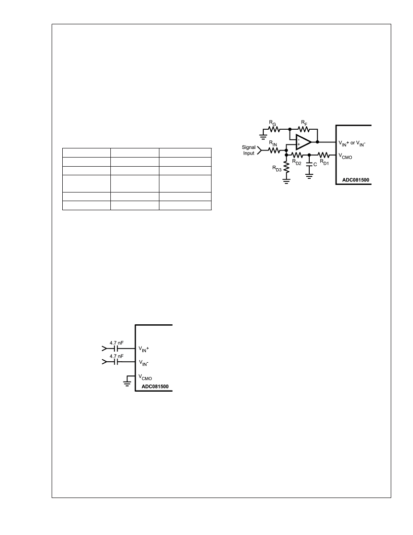
If d.c. coupling is used, it is best to servo the input common
mode voltage, using the V
CMO
pin, to maintain optimum
performance. An example of this type of circuit is shown in
Figure 12
.
One such circuit should be used in front of the V
IN
+ input and
another in front of the V
input. In that figure, R
, R
and
R
are used to divide the V
potential so that, after being
gained up by the amplifier, the input common mode voltage
is equal to V
from the ADC. R
and R
are split to
allow the bypass capacitor to isolate the input signal from
V
. R
, R
and R
will divide the input signal, if nec-
essary. If there is no need to divide the input signal, R
is not
needed. Capacitor "C" in
Figure 12
should be chosen to
keep any component of the input signal from affecting V
CMO
.
Be sure that the current drawn from the V
CMO
output does
not exceed 100 μA.
The Input impedance in the d.c. coupled mode (V
CMO
pin not
grounded) consists of a precision 100
resistor between
V
IN
+ and V
IN
and a capacitance from each of these inputs
to ground. In the a.c. coupled mode the input appears the
same except there is also a resistor of 50K between each
analog input pin and the V
CMO
potential.
Driving the inputs beyond full scale will result in a saturation
or clipping of the reconstructed output.
2.2.1 Handling Single-Ended Input Signals
There is no provision for the ADC081500 to adequately
process single-ended input signals. The best way to handle
single-ended signals is to convert them to differential signals
before presenting them to the ADC. The easiest way to
accomplish single-ended to differential signal conversion is
with an appropriate balun-connected transformer, as shown
in
Figure 13
.
20153144
FIGURE 11. Differential Input Drive
20153155
FIGURE 12. Example of Servoing the Analog Input with
V
CMO
A
www.national.com
22
相关PDF资料 |
PDF描述 |
|---|---|
| ADC081500CIYB | High Performance, Low Power, 8-Bit, 1.5 GSPS A/D Converter |
| ADC081500EVAL | High Performance, Low Power, 8-Bit, 1.5 GSPS A/D Converter |
| ADC08161 | 500 ns A/D Converter with S/H Function and 2.5V Bandgap Reference(500ns带S/H功能和2.5V带隙参考的A/D转换器) |
| ADC08161CIWM | 500 ns A/D Converter with S/H Function and 2.5V Bandgap Reference |
| ADC0816 | 8-BitμP Compatible A/D Converters with 16-Channel Multiplexer(带16通道多路器的8位μP兼容A/D转换器) |
相关代理商/技术参数 |
参数描述 |
|---|---|
| ADC081500_06 | 制造商:NSC 制造商全称:National Semiconductor 功能描述:High Performance, Low Power, 8-Bit, 1.5 GSPS A/D Converter |
| ADC081500_09 | 制造商:NSC 制造商全称:National Semiconductor 功能描述:High Performance, Low Power, 8-Bit, 1.5 GSPS A/D Converter |
| ADC081500CIYB | 功能描述:模数转换器 - ADC RoHS:否 制造商:Texas Instruments 通道数量:2 结构:Sigma-Delta 转换速率:125 SPs to 8 KSPs 分辨率:24 bit 输入类型:Differential 信噪比:107 dB 接口类型:SPI 工作电源电压:1.7 V to 3.6 V, 2.7 V to 5.25 V 最大工作温度:+ 85 C 安装风格:SMD/SMT 封装 / 箱体:VQFN-32 |
| ADC081500CIYB/NOPB | 功能描述:模数转换器 - ADC RoHS:否 制造商:Texas Instruments 通道数量:2 结构:Sigma-Delta 转换速率:125 SPs to 8 KSPs 分辨率:24 bit 输入类型:Differential 信噪比:107 dB 接口类型:SPI 工作电源电压:1.7 V to 3.6 V, 2.7 V to 5.25 V 最大工作温度:+ 85 C 安装风格:SMD/SMT 封装 / 箱体:VQFN-32 |
| ADC081500DEV | 制造商:NSC 制造商全称:National Semiconductor 功能描述:High Performance, Low Power, 8-Bit, 1.5 GSPS A/D Converter |
发布紧急采购,3分钟左右您将得到回复。