- 您现在的位置:买卖IC网 > PDF目录378277 > ADC081500 (National Semiconductor Corporation) High Performance, Low Power, 8-Bit, 1.5 GSPS A/D Converter PDF资料下载
参数资料
| 型号: | ADC081500 |
| 厂商: | National Semiconductor Corporation |
| 英文描述: | High Performance, Low Power, 8-Bit, 1.5 GSPS A/D Converter |
| 中文描述: | 高性能,低功耗,8位,1.5 GSPS的A / D转换 |
| 文件页数: | 27/28页 |
| 文件大小: | 830K |
| 代理商: | ADC081500 |
第1页第2页第3页第4页第5页第6页第7页第8页第9页第10页第11页第12页第13页第14页第15页第16页第17页第18页第19页第20页第21页第22页第23页第24页第25页第26页当前第27页第28页
2.0 Applications Information
(Continued)
input must exhibit low rms jitter. The allowable jitter is a
function of the input frequency and the input signal level, as
described in Section 2.3.
It is good practice to keep the ADC input clock line as short
as possible, to keep it well away from any other signals and
to treat it as a transmission line. Other signals can introduce
jitter into the input clock signal. The clock signal can also
introduce noise into the analog path if not isolated from that
path.
Best dynamic performance is obtained when the exposed
pad at the back of the package has a good connection to
ground. This is because this path from the die to ground is a
lower impedance than offered by the package pins.
2.9 USING THE SERIAL INTERFACE
The ADC081500 may be operated in the Normal control
mode (using control pins) or in the Extended control mode
(using a serial interface and register set).
Table 5
and
Table
6
describe the functions of pins 3, 4, 14 and 127 in the
Normal control mode and the Extended control mode, re-
spectively.
2.9.1 Normal Control Mode Operation
Normal control mode operation means that the Serial Inter-
face is not active and all controllable functions are controlled
with various pin settings. That is, the full-scale range, single-
ended or differential input and input coupling (a.c. or d.c.) are
all controlled with pin settings. The Normal control mode is
used by setting pin 14 high or low, as opposed to letting it
float.
Table 5
indicates the pin functions of theADC081500 in
the Normal control mode.
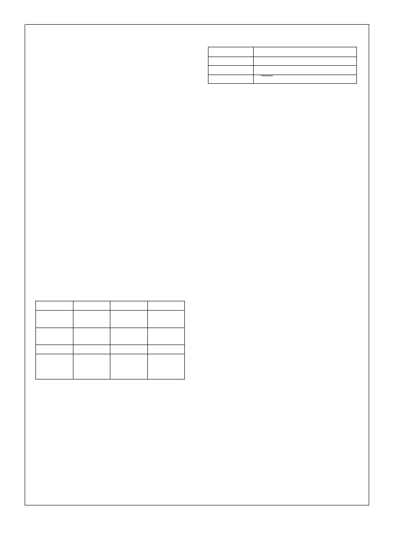
TABLE 5. Normal Control Mode Operation (Pin 14 High
or Low)
Pin
Low
High
0.70 V
P-P
Output
OutEdge =
Pos
CalDly High
Floating
3
0.50 V
P-P
Output
OutEdge =
Neg
CalDly Low
n/a
4
DDR
127
n/a
14
650 mV
P-P
input range
870 mV
P-P
input range
Extended
Control
Mode
Pin 3 can be either high or low in the Normal control mode.
Pin 14 must not be left floating to select this mode. See
Section 1.2 for more information.
Pin 4 can be high or low or can be left floating in the Normal
control mode. In the Normal control mode, pin 4 high or low
defines the edge at which the output data transitions. See
Section 2.4.3 for more information. If this pin is floating, the
output clock (DCLK) is a DDR (Double Data Rate) clock (see
Section 1.1.5.3) and the output edge synchronization is irrel-
evant since data is clocked out on both DCLK edges.
Pin 127, can be high or low in the Normal control mode, and
sets the calibration delay. Pin 127 is not designed to remain
floating.
TABLE 6. Extended Control Mode Operation (Pin 14
Floating)
Pin
3
4
127
Function
SCLK (Serial Clock)
SDATA (Serial Data)
SCS (Serial Interface Chip Select)
2.10 COMMON APPLICATION PITFALLS
Driving the inputs (analog or digital) beyond the power
supply rails.
For device reliability, no input should go more
than 150 mV below the ground pins or 150 mV above the
supply pins. Exceeding these limits on even a transient basis
may not only cause faulty or erratic operation, but may
impair device reliability. It is not uncommon for high speed
digital circuits to exhibit undershoot that goes more than a
volt below ground. Controlling the impedance of high speed
lines and terminating these lines in their characteristic im-
pedance should control overshoot.
Care should be taken not to overdrive the inputs of the
ADC081500. Such practice may lead to conversion inaccu-
racies and even to device damage.
Incorrect analog input common mode voltage in the d.c.
coupled mode.
As discussed in section 1.3 and 3.0, the
Input common mode voltage must remain within 50 mV of
the V
output , which has a variability with temperature
that must also be tracked. Distortion performance will be
degraded if the input common mode voltage is more than 50
mV from V
CMO
.
Using an inadequate amplifier to drive the analog input.
Use care when choosing a high frequency amplifier to drive
the ADC081500 as many high speed amplifiers will have
higher distortion than will the ADC081500, resulting in over-
all system performance degradation.
Driving the V
BG
pin to change the reference voltage.
As
mentioned in Section 2.1, the reference voltage is intended
to be fixed to provide one of two different full-scale values
(650 mV
and 870 mV
). Over driving this pin will not
change the full scale value, but can be used to change the
LVDS common mode voltage from 0.8V to 1.2V by tying the
V
BG
pin to V
A
.
Driving the clock input with an excessively high level
signal.
The ADC input clock level should not exceed the
level described in the Operating Ratings Table or the input
offset could change.
Inadequate input clock levels.
As described in Section 2.3,
insufficient input clock levels can result in poor performance.
Excessive input clock levels could result in the introduction
of an input offset.
Using a clock source with excessive jitter, using an
excessively long input clock signal trace, or having
other signals coupled to the input clock signal trace.
This will cause the sampling interval to vary, causing exces-
sive output noise and a reduction in SNR performance.
Failure to provide adequate heat removal.
As described in
Section 2.6.2, it is important to provide adequate heat re-
moval to ensure device reliability. This can either be done
with adequate air flow or the use of a simple heat sink built
into the board. The backside pad should be grounded for
best performance.
A
www.national.com
27
相关PDF资料 |
PDF描述 |
|---|---|
| ADC081500CIYB | High Performance, Low Power, 8-Bit, 1.5 GSPS A/D Converter |
| ADC081500EVAL | High Performance, Low Power, 8-Bit, 1.5 GSPS A/D Converter |
| ADC08161 | 500 ns A/D Converter with S/H Function and 2.5V Bandgap Reference(500ns带S/H功能和2.5V带隙参考的A/D转换器) |
| ADC08161CIWM | 500 ns A/D Converter with S/H Function and 2.5V Bandgap Reference |
| ADC0816 | 8-BitμP Compatible A/D Converters with 16-Channel Multiplexer(带16通道多路器的8位μP兼容A/D转换器) |
相关代理商/技术参数 |
参数描述 |
|---|---|
| ADC081500_06 | 制造商:NSC 制造商全称:National Semiconductor 功能描述:High Performance, Low Power, 8-Bit, 1.5 GSPS A/D Converter |
| ADC081500_09 | 制造商:NSC 制造商全称:National Semiconductor 功能描述:High Performance, Low Power, 8-Bit, 1.5 GSPS A/D Converter |
| ADC081500CIYB | 功能描述:模数转换器 - ADC RoHS:否 制造商:Texas Instruments 通道数量:2 结构:Sigma-Delta 转换速率:125 SPs to 8 KSPs 分辨率:24 bit 输入类型:Differential 信噪比:107 dB 接口类型:SPI 工作电源电压:1.7 V to 3.6 V, 2.7 V to 5.25 V 最大工作温度:+ 85 C 安装风格:SMD/SMT 封装 / 箱体:VQFN-32 |
| ADC081500CIYB/NOPB | 功能描述:模数转换器 - ADC RoHS:否 制造商:Texas Instruments 通道数量:2 结构:Sigma-Delta 转换速率:125 SPs to 8 KSPs 分辨率:24 bit 输入类型:Differential 信噪比:107 dB 接口类型:SPI 工作电源电压:1.7 V to 3.6 V, 2.7 V to 5.25 V 最大工作温度:+ 85 C 安装风格:SMD/SMT 封装 / 箱体:VQFN-32 |
| ADC081500DEV | 制造商:NSC 制造商全称:National Semiconductor 功能描述:High Performance, Low Power, 8-Bit, 1.5 GSPS A/D Converter |
发布紧急采购,3分钟左右您将得到回复。