- 您现在的位置:买卖IC网 > PDF目录1989 > ADF4350BCPZ-RL (Analog Devices Inc)IC SYNTH PLL VCO FN/IN 32LFCSP PDF资料下载
参数资料
| 型号: | ADF4350BCPZ-RL |
| 厂商: | Analog Devices Inc |
| 文件页数: | 17/32页 |
| 文件大小: | 0K |
| 描述: | IC SYNTH PLL VCO FN/IN 32LFCSP |
| 产品变化通告: | ADF4350, ADF4905/6 N-counter Change 05/Mar/2012 |
| 设计资源: | Broadband Low EVM Direct Conversion Transmitter (CN0134) Broadband Low EVM Direct Conversion Transmitter Using LO Divide-by-2 Modulator (CN0144) Using low noise linear drop-out regulators to power wideband PLL & VCO IC's (CN0147) |
| 标准包装: | 5,000 |
| 类型: | 扇出配送,分数-N,整数-N,时钟/频率合成器(RF) |
| PLL: | 是 |
| 输入: | CMOS,TTL |
| 输出: | 时钟 |
| 电路数: | 1 |
| 比率 - 输入:输出: | 1:3 |
| 差分 - 输入:输出: | 无/无 |
| 频率 - 最大: | 4.4GHz |
| 除法器/乘法器: | 是/是 |
| 电源电压: | 3 V ~ 3.6 V |
| 工作温度: | -40°C ~ 85°C |
| 安装类型: | 表面贴装 |
| 封装/外壳: | 32-VFQFN 裸露焊盘,CSP |
| 供应商设备封装: | 32-LFCSP-VQ(5x5) |
| 包装: | 带卷 (TR) |
第1页第2页第3页第4页第5页第6页第7页第8页第9页第10页第11页第12页第13页第14页第15页第16页当前第17页第18页第19页第20页第21页第22页第23页第24页第25页第26页第27页第28页第29页第30页第31页第32页
ADF4350
Rev. A | Page 24 of 32
SPUR CONSISTENCY AND FRACTIONAL SPUR
OPTIMIZATION
When a new frequency is programmed, the second sync pulse
after the LE rising edge is used to resynchronize the output
phase to the reference. The tSYNC time is to be programmed to
a value that is as least as long as the worst-case lock time. This
guarantees the phase resync occurs after the last cycle slip in the
PLL settling transient.
With dither off, the fractional spur pattern due to the quantiza-
tion noise of the SDM also depends on the particular phase
word with which the modulator is seeded.
The phase word can be varied to optimize the fractional and
subfractional spur levels on any particular frequency. Thus, a
look-up table of phase values corresponding to each frequency
can be constructed for use when programming the ADF4350.
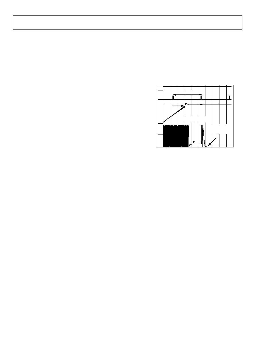
In the example shown in Figure 33, the PFD reference is 25 MHz
and MOD = 125 for a 200 kHz channel spacing. tSYNC is set to
400 μs by programming CLK_DIV_VALUE = 80.
LE
PHASE
FREQUENCY
SYNC
(INTERNAL)
–100
0
100
200
1000
300
400
500
600 700 800
900
0
73
25-
020
TIME (s)
PLL SETTLES TO
CORRECT PHASE
AFTER RESYNC
tSYNC
LAST CYCLE SLIP
PLL SETTLES TO
INCORRECT PHASE
If a look-up table is not used, keep the phase word at a constant
value to ensure consistent spur levels on any particular frequency.
PHASE RESYNC
The output of a fractional-N PLL can settle to any one of the
MOD phase offsets with respect to the input reference, where
MOD is the fractional modulus. The phase resync feature in the
ADF4350 produces a consistent output phase offset with respect
to the input reference. This is necessary in applications where the
output phase and frequency are important, such as digital beam
forming. See the Phase Programmability section to program a
specific RF output phase when using phase resync.
Phase resync is enabled by setting Bits [DB16:DB15] in
Register 3 to 1, 0. When phase resync is enabled, an internal
timer generates sync signals at intervals of tSYNC given by the
following formula:
Figure 33. Phase Resync Example
Phase Programmability
The phase word in Register 1 controls the RF output phase. As
this word is swept from 0 to MOD, the RF output phase sweeps
over a 360° range in steps of 360°/MOD.
tSYNC = CLK_DIV_VALUE × MOD × tPFD
where:
tPFD is the PFD reference period.
CLK_DIV_VALUE is the decimal value programmed in
Bits [DB14:DB3] of Register 3 and can be any integer in the
range of 1 to 4095.
MOD is the modulus value programmed in Bits [DB14:DB3] of
Register 1 (R1).
相关PDF资料 |
PDF描述 |
|---|---|
| ADF4351BCPZ | IC SYNTH PLL VCO 32LFCSP |
| ADF4360-0BCPZRL7 | IC SYNTHESIZER VCO 24LFCSP |
| ADF4360-1BCPZRL7 | IC SYNTHESIZER VCO 24LFCSP |
| ADF4360-2BCPZRL7 | IC SYNTHESIZER VCO 24LFCSP |
| ADF4360-3BCPZRL7 | IC SYNTHESIZER VCO 24LFCSP |
相关代理商/技术参数 |
参数描述 |
|---|---|
| ADF4350BCPZ-RL7 | 功能描述:IC SYNTH PLL VCO FN/IN 32LFCSP RoHS:是 类别:集成电路 (IC) >> 时钟/计时 - 时钟发生器,PLL,频率合成器 系列:- 标准包装:2,000 系列:- 类型:PLL 频率合成器 PLL:是 输入:晶体 输出:时钟 电路数:1 比率 - 输入:输出:1:1 差分 - 输入:输出:无/无 频率 - 最大:1GHz 除法器/乘法器:是/无 电源电压:4.5 V ~ 5.5 V 工作温度:-20°C ~ 85°C 安装类型:表面贴装 封装/外壳:16-LSSOP(0.175",4.40mm 宽) 供应商设备封装:16-SSOP 包装:带卷 (TR) 其它名称:NJW1504V-TE1-NDNJW1504V-TE1TR |
| ADF4350BCPZ-U6 | 制造商:Analog Devices 功能描述: |
| ADF4350EB1Z | 制造商:Analog Devices 功能描述:AD EVAL BOARD - Bulk |
| ADF4351 | 制造商:AD 制造商全称:Analog Devices 功能描述:Wideband Synthesizer |
| ADF4351BCPZ | 功能描述:IC SYNTH PLL VCO 32LFCSP RoHS:是 类别:集成电路 (IC) >> 时钟/计时 - 时钟发生器,PLL,频率合成器 系列:- 标准包装:2,000 系列:- 类型:PLL 时钟发生器 PLL:带旁路 输入:LVCMOS,LVPECL 输出:LVCMOS 电路数:1 比率 - 输入:输出:2:11 差分 - 输入:输出:是/无 频率 - 最大:240MHz 除法器/乘法器:是/无 电源电压:3.135 V ~ 3.465 V 工作温度:0°C ~ 70°C 安装类型:表面贴装 封装/外壳:32-LQFP 供应商设备封装:32-TQFP(7x7) 包装:带卷 (TR) |
发布紧急采购,3分钟左右您将得到回复。