- 您现在的位置:买卖IC网 > PDF目录1989 > ADF4350BCPZ-RL (Analog Devices Inc)IC SYNTH PLL VCO FN/IN 32LFCSP PDF资料下载
参数资料
| 型号: | ADF4350BCPZ-RL |
| 厂商: | Analog Devices Inc |
| 文件页数: | 19/32页 |
| 文件大小: | 0K |
| 描述: | IC SYNTH PLL VCO FN/IN 32LFCSP |
| 产品变化通告: | ADF4350, ADF4905/6 N-counter Change 05/Mar/2012 |
| 设计资源: | Broadband Low EVM Direct Conversion Transmitter (CN0134) Broadband Low EVM Direct Conversion Transmitter Using LO Divide-by-2 Modulator (CN0144) Using low noise linear drop-out regulators to power wideband PLL & VCO IC's (CN0147) |
| 标准包装: | 5,000 |
| 类型: | 扇出配送,分数-N,整数-N,时钟/频率合成器(RF) |
| PLL: | 是 |
| 输入: | CMOS,TTL |
| 输出: | 时钟 |
| 电路数: | 1 |
| 比率 - 输入:输出: | 1:3 |
| 差分 - 输入:输出: | 无/无 |
| 频率 - 最大: | 4.4GHz |
| 除法器/乘法器: | 是/是 |
| 电源电压: | 3 V ~ 3.6 V |
| 工作温度: | -40°C ~ 85°C |
| 安装类型: | 表面贴装 |
| 封装/外壳: | 32-VFQFN 裸露焊盘,CSP |
| 供应商设备封装: | 32-LFCSP-VQ(5x5) |
| 包装: | 带卷 (TR) |
第1页第2页第3页第4页第5页第6页第7页第8页第9页第10页第11页第12页第13页第14页第15页第16页第17页第18页当前第19页第20页第21页第22页第23页第24页第25页第26页第27页第28页第29页第30页第31页第32页
ADF4350
Rev. A | Page 26 of 32
INTERFACING
The ADF4350 has a simple SPI-compatible serial interface for
writing to the device. CLK, DATA, and LE control the data
transfer. When LE goes high, the 32 bits that have been clocked
into the appropriate register on each rising edge of CLK are
transferred to the appropriate latch. See Figure 2 for the timing
diagram and Table 5 for the register address table.
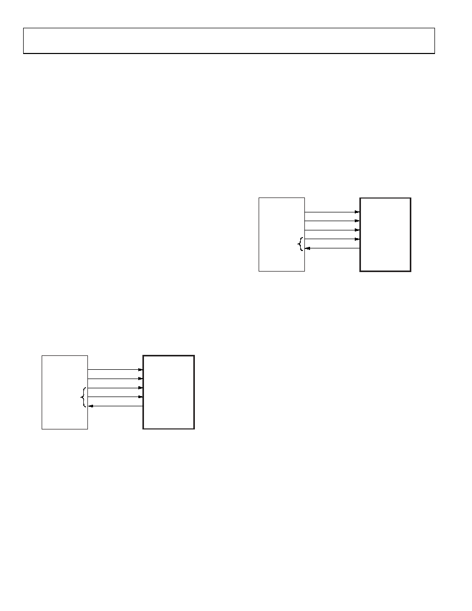
ADuC70xx Interface
Figure 35 shows the interface between the ADF4350 and the
ADuC70xx family of analog microcontrollers. The ADuC70xx
family is based on an AMR7 core, although the same interface
can be used with any 8051-based microcontroller. The micro-
controller is set up for SPI master mode with CPHA = 0. To
initiate the operation, the I/O port driving LE is brought low.
Each latch of the ADF4350 needs a 32-bit word. This is accom-
plished by writing four 8-bit bytes from the microcontroller to
the device. When the last byte is written, the LE input should be
brought high to complete the transfer.
On first applying power to the ADF4350, it needs six writes
(one each to R5, R4, R3, R2, R1, R0) for the output to become
active.
I/O port lines on the microcontroller are also used to control
power-down (CE input) and to detect lock (MUXOUT
configured as lock detect and polled by the port input).
When operating in the mode described, the maximum SPI
transfer rate of the ADuC7023 is 20 Mbps. This means that
the maximum rate at which the output frequency can be
changed is 833 kHz. If using a faster SPI clock just make sure
the SPI timing requirements listed in Table 2 are adhered to.
07
32
5-
02
2
ADuC70xx
ADF4350
CLK
DATA
LE
CE
MUXOUT
(LOCK DETECT)
SCLOCK
MOSI
I/O PORTS
Figure 35. ADuC812 to ADF4350 Interface
ADSP-BF527 Interface
Figure 36 shows the interface between the ADF4351 and the
Blackfin ADSP-BF527 digital signal processor (DSP). The
ADF4351 needs a 32-bit serial word for each latch write. The
easiest way to accomplish this using the Blackfin family is to use
the autobuffered transmit mode of operation with alternate
framing. This provides a means for transmitting an entire block
of serial data before an interrupt is generated. Set up the word
length for 8 bits and use three memory locations for each 32-bit
word. To program each 32-bit latch, store the four 8-bit bytes,
enable the autobuffered mode, and write to the transmit register
of the DSP. This last operation initiates the autobuffer transfer.
Make sure the clock speeds are within the maximum limits
outlined in Table 2.
07
32
5-
02
3
ADSP-BF527
ADF4350
CLK
DATA
LE
CE
MUXOUT
(LOCK DETECT)
SCK
MOSI
GPIO
I/O FLAGS
Figure 36. ADSP-BF527 to ADF4350 Interface
PCB DESIGN GUIDELINES FOR A CHIP SCALE
PACKAGE
The lands on the chip scale package (CP-32-2) are rectangular.
The PCB pad for these is to be 0.1 mm longer than the package
land length and 0.05 mm wider than the package land width.
The land is to be centered on the pad. This ensures the solder
joint size is maximized. The bottom of the chip scale package
has a central thermal pad.
The thermal pad on the PCB is to be at least as large as the
exposed pad. On the PCB, there is to be a minimum clearance
of 0.25 mm between the thermal pad and the inner edges of the
pad pattern. This ensures that shorting is avoided.
Thermal vias can be used on the PCB thermal pad to improve
the thermal performance of the package. If vias are used, they
are to be incorporated in the thermal pad at 1.2 mm pitch grid.
The via diameter is to be between 0.3 mm and 0.33 mm, and the
via barrel is to be plated with 1 oz. of copper to plug the via.
相关PDF资料 |
PDF描述 |
|---|---|
| ADF4351BCPZ | IC SYNTH PLL VCO 32LFCSP |
| ADF4360-0BCPZRL7 | IC SYNTHESIZER VCO 24LFCSP |
| ADF4360-1BCPZRL7 | IC SYNTHESIZER VCO 24LFCSP |
| ADF4360-2BCPZRL7 | IC SYNTHESIZER VCO 24LFCSP |
| ADF4360-3BCPZRL7 | IC SYNTHESIZER VCO 24LFCSP |
相关代理商/技术参数 |
参数描述 |
|---|---|
| ADF4350BCPZ-RL7 | 功能描述:IC SYNTH PLL VCO FN/IN 32LFCSP RoHS:是 类别:集成电路 (IC) >> 时钟/计时 - 时钟发生器,PLL,频率合成器 系列:- 标准包装:2,000 系列:- 类型:PLL 频率合成器 PLL:是 输入:晶体 输出:时钟 电路数:1 比率 - 输入:输出:1:1 差分 - 输入:输出:无/无 频率 - 最大:1GHz 除法器/乘法器:是/无 电源电压:4.5 V ~ 5.5 V 工作温度:-20°C ~ 85°C 安装类型:表面贴装 封装/外壳:16-LSSOP(0.175",4.40mm 宽) 供应商设备封装:16-SSOP 包装:带卷 (TR) 其它名称:NJW1504V-TE1-NDNJW1504V-TE1TR |
| ADF4350BCPZ-U6 | 制造商:Analog Devices 功能描述: |
| ADF4350EB1Z | 制造商:Analog Devices 功能描述:AD EVAL BOARD - Bulk |
| ADF4351 | 制造商:AD 制造商全称:Analog Devices 功能描述:Wideband Synthesizer |
| ADF4351BCPZ | 功能描述:IC SYNTH PLL VCO 32LFCSP RoHS:是 类别:集成电路 (IC) >> 时钟/计时 - 时钟发生器,PLL,频率合成器 系列:- 标准包装:2,000 系列:- 类型:PLL 时钟发生器 PLL:带旁路 输入:LVCMOS,LVPECL 输出:LVCMOS 电路数:1 比率 - 输入:输出:2:11 差分 - 输入:输出:是/无 频率 - 最大:240MHz 除法器/乘法器:是/无 电源电压:3.135 V ~ 3.465 V 工作温度:0°C ~ 70°C 安装类型:表面贴装 封装/外壳:32-LQFP 供应商设备封装:32-TQFP(7x7) 包装:带卷 (TR) |
发布紧急采购,3分钟左右您将得到回复。