- 您现在的位置:买卖IC网 > PDF目录1989 > ADF4350BCPZ-RL (Analog Devices Inc)IC SYNTH PLL VCO FN/IN 32LFCSP PDF资料下载
参数资料
| 型号: | ADF4350BCPZ-RL |
| 厂商: | Analog Devices Inc |
| 文件页数: | 30/32页 |
| 文件大小: | 0K |
| 描述: | IC SYNTH PLL VCO FN/IN 32LFCSP |
| 产品变化通告: | ADF4350, ADF4905/6 N-counter Change 05/Mar/2012 |
| 设计资源: | Broadband Low EVM Direct Conversion Transmitter (CN0134) Broadband Low EVM Direct Conversion Transmitter Using LO Divide-by-2 Modulator (CN0144) Using low noise linear drop-out regulators to power wideband PLL & VCO IC's (CN0147) |
| 标准包装: | 5,000 |
| 类型: | 扇出配送,分数-N,整数-N,时钟/频率合成器(RF) |
| PLL: | 是 |
| 输入: | CMOS,TTL |
| 输出: | 时钟 |
| 电路数: | 1 |
| 比率 - 输入:输出: | 1:3 |
| 差分 - 输入:输出: | 无/无 |
| 频率 - 最大: | 4.4GHz |
| 除法器/乘法器: | 是/是 |
| 电源电压: | 3 V ~ 3.6 V |
| 工作温度: | -40°C ~ 85°C |
| 安装类型: | 表面贴装 |
| 封装/外壳: | 32-VFQFN 裸露焊盘,CSP |
| 供应商设备封装: | 32-LFCSP-VQ(5x5) |
| 包装: | 带卷 (TR) |
第1页第2页第3页第4页第5页第6页第7页第8页第9页第10页第11页第12页第13页第14页第15页第16页第17页第18页第19页第20页第21页第22页第23页第24页第25页第26页第27页第28页第29页当前第30页第31页第32页
ADF4350
Rev. A | Page 7 of 32
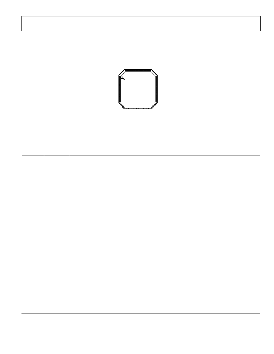
PIN CONFIGURATION AND FUNCTION DESCRIPTIONS
1
CLK
2
DATA
3
LE
4
CE
5
SW
6
7
24
VREF
23
VCOM
22
21
20
19
18
17
8
SD
V
DD
ADF4350
TOP VIEW
(Not to Scale)
9
AG
ND
10
AV
DD
11
RE
F
IN
12
DG
ND
13
DV
DD
14
15
16
32
31
30
29
28
SD
GN
D
27
26
25
PIN 1
INDICATOR
VP
CPOUT
CPGND
MU
X
O
U
T
RSET
RF
OU
T
A+
RF
OU
T
B+
RF
OU
T
B
RF
OU
T
A
V
VCO
VTUNE
AGNDVCO
TEMP
PD
B
RF
LD
A
GN
D
V
C
O
VVCO
073
25
-00
3
NOTES
1. THE LFCSP HAS AN EXPOSED PADDLE THAT MUST BE CONNECTED TO GND.
Figure 3. Pin Configuration
Table 4. Pin Function Descriptions
Pin No.
Mnemonic
Description
1
CLK
Serial Clock Input. Data is clocked into the 32-bit shift register on the CLK rising edge. This input is a high
impedance CMOS input.
2
DATA
Serial Data Input. The serial data is loaded MSB first with the three LSBs as the control bits. This input is a high
impedance CMOS input.
3
LE
Load Enable, CMOS Input. When LE goes high, the data stored in the shift register is loaded into the register
that is selected by the three LSBs.
4
CE
Chip Enable. A logic low on this pin powers down the device and puts the charge pump into three-state mode.
A logic high on this pin powers up the device depending on the status of the power-down bits.
5
SW
Fast-Lock Switch. A connection should be made from the loop filter to this pin when using the fast-lock mode.
6
VP
Charge Pump Power Supply. This pin is to be equal to AVDD. Decoupling capacitors to the ground plane are to
be placed as close as possible to this pin.
7
CPOUT
Charge Pump Output. When enabled, this provides ±ICP to the external loop filter. The output of the loop filter is
connected to VTUNE to drive the internal VCO.
8
CPGND
Charge Pump Ground. This is the ground return pin for CPOUT.
9
AGND
Analog Ground. This is a ground return pin for AVDD.
10
AVDD
Analog Power Supply. This pin ranges from 3.0 V to 3.6 V. Decoupling capacitors to the analog ground plane are
to be placed as close as possible to this pin. AVDD must have the same value as DVDD.
11, 18, 21
AGNDVCO
VCO Analog Ground. These are the ground return pins for the VCO.
12
RFOUTA+
VCO Output. The output level is programmable. The VCO fundamental output or a divided down version is available.
13
RFOUTA
Complementary VCO Output. The output level is programmable. The VCO fundamental output or a divided
down version is available.
14
RFOUTB+
Auxilliary VCO Output. The output level is programmable. The VCO fundamental output or a divided down
version is available.
15
RFOUTB
Complementary Auxilliary VCO Output. The output level is programmable. The VCO fundamental output or a
divided down version is available.
16, 17
VVCO
Power Supply for the VCO. This ranges from 3.0 V to 3.6 V. Decoupling capacitors to the analog ground plane
should be placed as close as possible to these pins. VVCO must have the same value as AVDD.
19
TEMP
Temperature Compensation Output. Decoupling capacitors to the ground plane are to be placed as close as
possible to this pin.
20
VTUNE
Control Input to the VCO. This voltage determines the output frequency and is derived from filtering the CPOUT
output voltage.
相关PDF资料 |
PDF描述 |
|---|---|
| ADF4351BCPZ | IC SYNTH PLL VCO 32LFCSP |
| ADF4360-0BCPZRL7 | IC SYNTHESIZER VCO 24LFCSP |
| ADF4360-1BCPZRL7 | IC SYNTHESIZER VCO 24LFCSP |
| ADF4360-2BCPZRL7 | IC SYNTHESIZER VCO 24LFCSP |
| ADF4360-3BCPZRL7 | IC SYNTHESIZER VCO 24LFCSP |
相关代理商/技术参数 |
参数描述 |
|---|---|
| ADF4350BCPZ-RL7 | 功能描述:IC SYNTH PLL VCO FN/IN 32LFCSP RoHS:是 类别:集成电路 (IC) >> 时钟/计时 - 时钟发生器,PLL,频率合成器 系列:- 标准包装:2,000 系列:- 类型:PLL 频率合成器 PLL:是 输入:晶体 输出:时钟 电路数:1 比率 - 输入:输出:1:1 差分 - 输入:输出:无/无 频率 - 最大:1GHz 除法器/乘法器:是/无 电源电压:4.5 V ~ 5.5 V 工作温度:-20°C ~ 85°C 安装类型:表面贴装 封装/外壳:16-LSSOP(0.175",4.40mm 宽) 供应商设备封装:16-SSOP 包装:带卷 (TR) 其它名称:NJW1504V-TE1-NDNJW1504V-TE1TR |
| ADF4350BCPZ-U6 | 制造商:Analog Devices 功能描述: |
| ADF4350EB1Z | 制造商:Analog Devices 功能描述:AD EVAL BOARD - Bulk |
| ADF4351 | 制造商:AD 制造商全称:Analog Devices 功能描述:Wideband Synthesizer |
| ADF4351BCPZ | 功能描述:IC SYNTH PLL VCO 32LFCSP RoHS:是 类别:集成电路 (IC) >> 时钟/计时 - 时钟发生器,PLL,频率合成器 系列:- 标准包装:2,000 系列:- 类型:PLL 时钟发生器 PLL:带旁路 输入:LVCMOS,LVPECL 输出:LVCMOS 电路数:1 比率 - 输入:输出:2:11 差分 - 输入:输出:是/无 频率 - 最大:240MHz 除法器/乘法器:是/无 电源电压:3.135 V ~ 3.465 V 工作温度:0°C ~ 70°C 安装类型:表面贴装 封装/外壳:32-LQFP 供应商设备封装:32-TQFP(7x7) 包装:带卷 (TR) |
发布紧急采购,3分钟左右您将得到回复。