- 您现在的位置:买卖IC网 > PDF目录1775 > ADM1066ASUZ-REEL7 (Analog Devices Inc)IC SEQUENCER/SUPERVISOR 48TQFP PDF资料下载
参数资料
| 型号: | ADM1066ASUZ-REEL7 |
| 厂商: | Analog Devices Inc |
| 文件页数: | 15/32页 |
| 文件大小: | 0K |
| 描述: | IC SEQUENCER/SUPERVISOR 48TQFP |
| 标准包装: | 500 |
| 系列: | Super Sequencer® |
| 类型: | 序列发生器 |
| 监视电压数目: | 12 |
| 输出: | 可编程 |
| 电压 - 阀值: | 可调节/可选择 |
| 工作温度: | -40°C ~ 85°C |
| 安装类型: | 表面贴装 |
| 封装/外壳: | 48-TQFP |
| 供应商设备封装: | 48-TQFP(7x7) |
| 包装: | 带卷 (TR) |
| 配用: | EVAL-ADM1066TQEBZ-ND - BOARD EVALUATION FOR ADM1066TQ |
第1页第2页第3页第4页第5页第6页第7页第8页第9页第10页第11页第12页第13页第14页当前第15页第16页第17页第18页第19页第20页第21页第22页第23页第24页第25页第26页第27页第28页第29页第30页第31页第32页
�� ��
��
��ADM1066�
�INPUTS�
�SUPPLY� SUPERVISION�
�The� ADM1066� has� 10� programmable� inputs.� Five� of� these� are�
�dedicated� supply� fault� detectors� (SFDs).� These� dedicated� inputs�
�are� called� VH� and� VPx� (VP1� to� VP4)� by� default.� The� other� five�
�inputs� are� labeled� VXx� (VX1� to� VX5)� and� have� dual� functionality.�
�They� can� be� used� either� as� SFDs,� with� functionality� similar� to� that�
�of� VH� and� VPx,� or� as� CMOS-/TTL-compatible� logic� inputs� to�
�the� device.� Therefore,� the� ADM1066� can� have� up� to� 10� analog�
�inputs,� a� minimum� of� five� analog� inputs� and� five� digital� inputs,�
�or� a� combination� thereof.� If� an� input� is� used� as� an� analog� input,�
�it� cannot� be� used� as� a� digital� input.� Therefore,� a� configuration�
��shows� the� details� of� each� input.�
�PROGRAMMING� THE� SUPPLY� FAULT� DETECTORS�
�The� ADM1066� can� have� up� to� 10� SFDs� on� its� 10� input� channels.�
�These� highly� programmable� reset� generators� enable� the� supervision�
�of� up� to� 10� supply� voltages.� The� supplies� can� be� as� low� as� 0.573� V�
�and� as� high� as� 14.4� V.� The� inputs� can� be� configured� to� detect� an�
�undervoltage� fault� (the� input� voltage� drops� below� a� prepro-�
�grammed� value),� an� overvoltage� fault� (the� input� voltage� rises�
�above� a� preprogrammed� value),� or� an� out-of-window� fault� (the�
�input� voltage� is� outside� a� preprogrammed� range).� The� thresholds�
�can� be� programmed� to� an� 8-bit� resolution� in� registers� provided� in�
�The� threshold� value� required� is� given� by�
�V� T� =� (� V� R� � N� )/255� +� V� B�
�where:�
�V� T� is� the� desired� threshold� voltage� (undervoltage� or� overvoltage).�
�V� R� is� the� voltage� range.�
�N� is� the� decimal� value� of� the� 8-bit� code.�
�V� B� is� the� bottom� of� the� range.�
�Reversing� the� equation,� the� code� for� a� desired� threshold� is� given� by�
�N� =� 255� � (� V� T� ?� V� B� )/� V� R�
�For� example,� if� the� user� wants� to� set� a� 5� V� overvoltage� threshold�
�on� VP1,� the� code� to� be� programmed� in� the� PS1OVTH� register�
�(as� discussed� in� the� AN-698� Application� Note� at� www.analog.com� )�
�is� given� by�
�N� =� 255� � (5� ?� 2.5)/3.5�
�Therefore,� N� =� 182� (1011� 0110� or� 0xB6).�
�INPUT� COMPARATOR� HYSTERESIS�
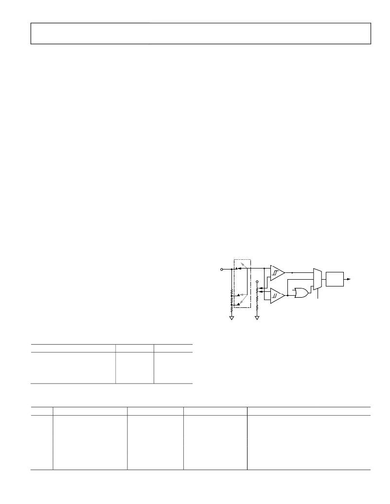
�The� UV� and� OV� comparators� shown� in� Figure� 22� are� always�
�looking� at� VPx.� To� avoid� chatter� (multiple� transitions� when� the�
�input� is� very� close� to� the� set� threshold� level),� these� comparators�
�have� digitally� programmable� hysteresis.� The� hysteresis� can� be�
��the� ADM1066.� This� translates� to� a� voltage� resolution� that� is�
�dependent� on� the� range� selected.�
�The� resolution� is� given� by�
�Step� Size� =� Threshold� Range� /255�
�VPx�
�ULTRA�
�LOW�
�RANGE�
�SELECT�
�VREF�
�+�
�–�
�OV�
�COMPARATOR�
�GLITCH�
�FILTER�
�FAULT�
�OUTPUT�
�Therefore,� if� the� high� range� is� selected� on� VH,� the� step� size� can�
�+�
�be� calculated� as� follows:�
�(14.4� V� ?� 6.0� V)/255� =� 32.9� mV�
�LOW�
�MID�
�–�
�UV�
�COMPARATOR�
�FAULT� TYPE�
�SELECT�
��the� bottom� of� each� range� (V� B� ),� and� the� range� itself� (V� R� ).�
�Figure� 22.� Supply� Fault� Detector� Block�
�Table� 5.� Voltage� Range� Limits�
�Voltage� Range� (V)�
�0.573� to� 1.375�
�1.25� to� 3.00�
�2.5� to� 6.0�
�6.0� to� 14.4�
�V� B� (V)�
�0.573�
�1.25�
�2.5�
�6.0�
�V� R� (V)�
�0.802�
�1.75�
�3.5�
�8.4�
�The� hysteresis� is� added� after� a� supply� voltage� goes� out� of�
�tolerance.� Therefore,� the� user� can� program� the� amount� above�
�the� undervoltage� threshold� to� which� the� input� must� rise� before�
�an� undervoltage� fault� is� deasserted.� Similarly,� the� user� can� program�
�the� amount� below� the� overvoltage� threshold� to� which� an� input�
�must� fall� before� an� overvoltage� fault� is� deasserted.�
�Table� 6.� Input� Functions,� Thresholds,� and� Ranges�
�Input�
�VH�
�VPx�
�VXx�
�Function�
�High� Voltage� Analog� Input�
�Positive� Analog� Input�
�High-Z� Analog� Input�
�Digital� Input�
�Voltage� Range� (V)�
�2.5� to� 6.0�
�6.0� to� 14.4�
�0.573� to� 1.375�
�1.25� to� 3.00�
�2.5� to� 6.0�
�0.573� to� 1.375�
�0� to� 5.0�
�Maximum� Hysteresis�
�425� mV�
�1.02� V�
�97.5� mV�
�212� mV�
�425� mV�
�97.5� mV�
�N/A�
�Voltage� Resolution� (mV)�
�13.7�
�32.9�
�3.14�
�6.8�
�13.7�
�3.14�
�N/A�
�Glitch� Filter� (μs)�
�0� to� 100�
�0� to� 100�
�0� to� 100�
�0� to� 100�
�0� to� 100�
�0� to� 100�
�0� to� 100�
�Rev.� E� |� Page� 15� of� 32�
�相关PDF资料 |
PDF描述 |
|---|---|
| ADM1067ACPZ | IC SEQUENCER/SUPERVISOR 40-LFCSP |
| ADM1068ASTZ-REEL7 | IC SEQUENCER/SUPERVISOR 32LQFP |
| ADM1069ACPZ-REEL7 | IC SUPERVISOR/SEQ PROG 40LFCSP |
| ADM1088AKS-REEL7 | IC SIMPLE SEQUENCER P-P SC70-6 |
| ADM1169ASTZ | IC SEQUENCER/SUPERVISOR 32LQFP |
相关代理商/技术参数 |
参数描述 |
|---|---|
| ADM1067 | 制造商:AD 制造商全称:Analog Devices 功能描述:Super Sequencer with Open-Loop Margining DACs |
| ADM1067ACP | 制造商:Analog Devices 功能描述:Sequencer 40-Pin LFCSP EP |
| ADM1067ACP-REEL | 制造商:Analog Devices 功能描述:Sequencer 40-Pin LFCSP EP T/R |
| ADM1067ACP-REEL7 | 制造商:Analog Devices 功能描述:Sequencer 40-Pin LFCSP EP T/R |
| ADM1067ACPZ | 功能描述:IC SEQUENCER/SUPERVISOR 40-LFCSP RoHS:是 类别:集成电路 (IC) >> PMIC - 监控器 系列:Super Sequencer® 标准包装:1 系列:- 类型:简单复位/加电复位 监视电压数目:1 输出:开路漏极或开路集电极 复位:高有效 复位超时:- 电压 - 阀值:1.8V 工作温度:-40°C ~ 125°C 安装类型:表面贴装 封装/外壳:6-TSOP(0.059",1.50mm 宽)5 引线 供应商设备封装:5-TSOP 包装:剪切带 (CT) 其它名称:NCP301HSN18T1GOSCT |
发布紧急采购,3分钟左右您将得到回复。