- 您现在的位置:买卖IC网 > PDF目录1775 > ADM1066ASUZ-REEL7 (Analog Devices Inc)IC SEQUENCER/SUPERVISOR 48TQFP PDF资料下载
参数资料
| 型号: | ADM1066ASUZ-REEL7 |
| 厂商: | Analog Devices Inc |
| 文件页数: | 23/32页 |
| 文件大小: | 0K |
| 描述: | IC SEQUENCER/SUPERVISOR 48TQFP |
| 标准包装: | 500 |
| 系列: | Super Sequencer® |
| 类型: | 序列发生器 |
| 监视电压数目: | 12 |
| 输出: | 可编程 |
| 电压 - 阀值: | 可调节/可选择 |
| 工作温度: | -40°C ~ 85°C |
| 安装类型: | 表面贴装 |
| 封装/外壳: | 48-TQFP |
| 供应商设备封装: | 48-TQFP(7x7) |
| 包装: | 带卷 (TR) |
| 配用: | EVAL-ADM1066TQEBZ-ND - BOARD EVALUATION FOR ADM1066TQ |
第1页第2页第3页第4页第5页第6页第7页第8页第9页第10页第11页第12页第13页第14页第15页第16页第17页第18页第19页第20页第21页第22页当前第23页第24页第25页第26页第27页第28页第29页第30页第31页第32页
�� �
�
�ADM1066�
�VIN�
�ADM1066�
�MICROCONTROLLER�
�DC-TO-DC�
�CONVERTER�
�OUTPUT�
�FEEDBACK�
�R1�
�ATTENUATION�
�RESISTOR,� R3�
�VH/VPx/VXx�
�DACx�
�MUX�
�ADC�
�DAC�
�DEVICE�
�CONTROLLER�
�(SMBus)�
�GND�
�R2�
�PCB�
�TRACE� NOISE�
�DECOUPLING�
�CAPACITOR�
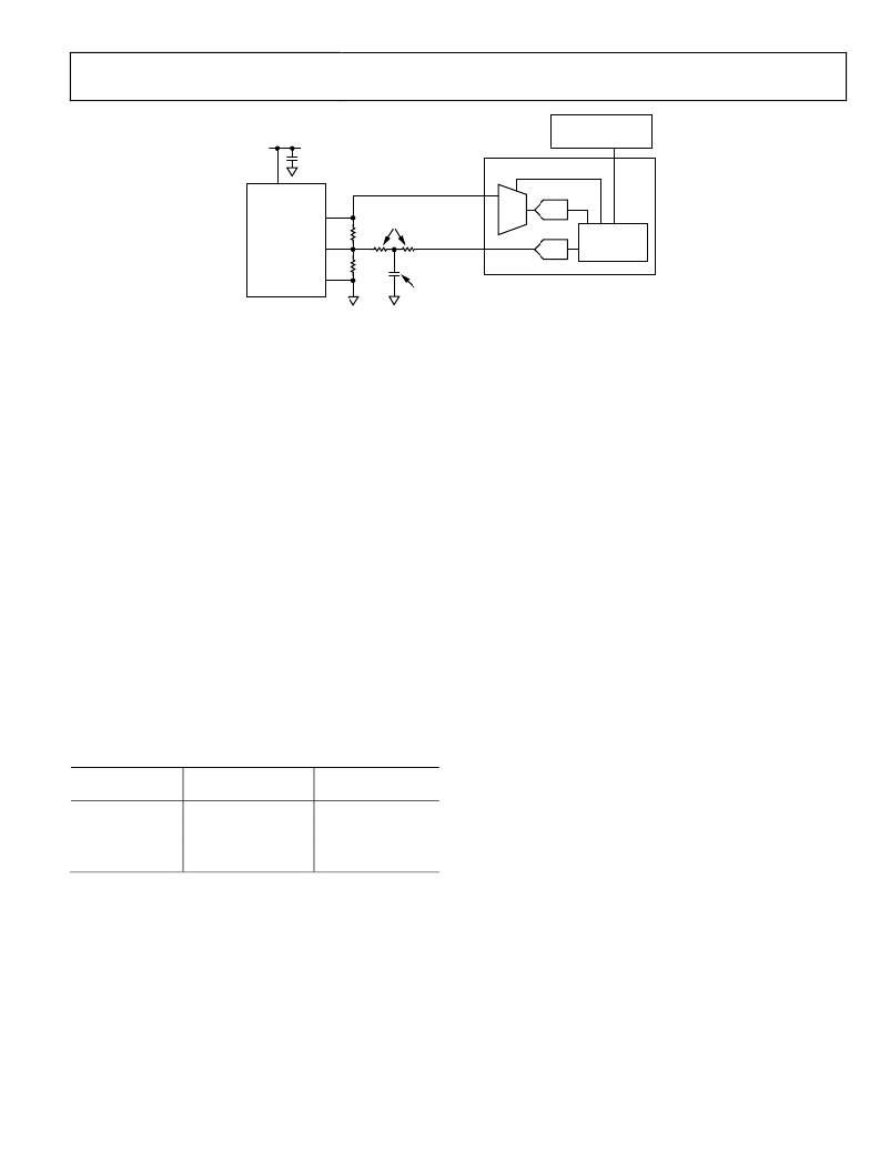
�Figure� 33.� Closed-Loop� Margining� System� Using� the� ADM1066�
�WRITING� TO� THE� DACs�
�Four� DAC� ranges� are� offered.� They� can� be� placed� with� midcode�
�(Code� 0x7F)� at� 0.6� V,� 0.8� V,� 1.0� V,� and� 1.25� V.� These� voltages� are�
�Therefore,� a� direct� relationship� exists� between� the� extra� voltage�
�drop� across� R1� during� margining� and� the� voltage� drop� across� R3.�
�This� relationship� is� given� by� the� following� equation:�
�placed� to� correspond� to� the� most� common� feedback� voltages.�
�Centering� the� DAC� outputs� in� this� way� provides� the� best� use� of�
�Δ� V� OUT� =�
�R1�
�R3�
�(� V� FB� ?� V� DACOUT� )�
�the� DAC� resolution.� For� most� supplies,� it� is� possible� to� place� the�
�DAC� midcode� at� the� point� where� the� dc-to-dc� converter� output�
�is� not� modified,� thereby� giving� half� of� the� DAC� range� to� margin�
�up� and� the� other� half� to� margin� down.�
�The� DAC� output� voltage� is� set� by� the� code� written� to� the� DACx�
�register.� The� voltage� is� linear� with� the� unsigned� binary� number�
�in� this� register.� Code� 0x7F� is� placed� at� the� midcode� voltage,� as�
�described� previously.� The� output� voltage� is� given� by�
�DAC� Output� =� (� DACx� ?� 0x7F)/255� � 0.6015� +� V� OFF�
�where� V� OFF� is� one� of� the� four� offset� voltages.�
�There� are� 256� DAC� settings� available.� The� midcode� value� is�
�located� at� DAC� Code� 0x7F� as� close� as� possible� to� the� middle�
�of� the� 256� code� range.� The� full� output� swing� of� the� DACs� is�
�+302� mV� (+128� codes)� and� ?300� mV� (?127� codes)� around� the�
�selected� midcode� voltage.� The� voltage� range� for� each� midcode�
��where:�
�Δ� V� OUT� is� the� change� in� V� OUT� .�
�V� FB� is� the� voltage� at� the� feedback� node� of� the� dc-to-dc� converter.�
�V� DACOUT� is� the� voltage� output� of� the� margining� DAC.�
�This� equation� demonstrates� that� if� the� user� wants� the� output�
�voltage� to� change� by� ±300� mV,� then� R1� =� R3.� If� the� user� wants� the�
�output� voltage� to� change� by� ±600� mV,� R1� =� 2� ×� R3,� and� so� on.�
�It� is� best� to� use� the� full� DAC� output� range� to� margin� a� supply.�
�Choosing� the� attenuation� resistor� in� this� way� provides� the� most�
�resolution� from� the� DAC,� meaning� that� with� one� DAC� code�
�change,� the� smallest� effect� on� the� dc-to-dc� converter� output�
�voltage� is� induced.� If� the� resistor� is� sized� up� to� use� a� code� such�
�as� 27� decimal� to� 227� decimal� to� move� the� dc-to-dc� converter� output�
�by� ±5%,� it� takes� 100� codes� to� move� 5%� (each� code� moves� the�
�output� by� 0.05%).� This� is� beyond� the� readback� accuracy� of� the�
�ADC,� but� it� should� not� prevent� the� user� from� building� a� circuit�
�to� use� the� most� resolution.�
�Table� 10.� Ranges� for� Midcode� Voltages�
�Midcode� Minimum� Voltage�
�Maximum� Voltage�
�DAC� LIMITING� AND� OTHER� SAFETY� FEATURES�
�Voltage� (V)�
�0.6�
�0.8�
�1.0�
�1.25�
�Output� (V)�
�0.300�
�0.500�
�0.700�
�0.950�
�Output� (V)�
�0.902�
�1.102�
�1.302�
�1.552�
�Limit� registers� (called� DPLIMx� and� DNLIMx)� on� the� device�
�offer� the� user� some� protection� from� firmware� bugs� that� can�
�cause� catastrophic� board� problems� by� forcing� supplies� beyond�
�their� allowable� output� ranges.� Essentially,� the� DAC� code� written�
�into� the� DACx� register� is� clipped� such� that� the� code� used� to� set�
�the� DAC� voltage� is� given� by�
�CHOOSING� THE� SIZE� OF� THE� ATTENUATION�
�DAC� Code�
�RESISTOR�
�The� size� of� the� attenuation� resistor,� R3,� determines� how� much�
�the� DAC� voltage� swing� affects� the� output� voltage� of� the� dc-to-dc�
�=� DACx,�
�=� DNLIMx,�
�=� DPLIMx,�
�DACx� ≥� DNLIMx� and� DACx� ≤� DPLIMx�
�DACx� <� DNLIMx�
�DACx� >� DPLIMx�
�converter� that� is� being� margined� (see� Figure� 33).�
�Because� the� voltage� at� the� feedback� pin� remains� constant,� the�
�current� flowing� from� the� feedback� node� to� GND� through� R2� is�
�a� constant.� In� addition,� the� feedback� node� itself� is� high� impedance.�
�This� means� that� the� current� flowing� through� R1� is� the� same� as�
�the� current� flowing� through� R3.�
�In� addition,� the� DAC� output� buffer� is� three-stated� if�
�DNLIMx� >� DPLIMx.� By� programming� the� limit� registers�
�this� way,� the� user� can� make� it� very� difficult� for� the� DAC�
�output� buffers� to� be� turned� on� during� normal� system� operation.�
�The� limit� registers� are� among� the� registers� downloaded� from�
�EEPROM� at� startup.�
�Rev.� E� |� Page� 23� of� 32�
�相关PDF资料 |
PDF描述 |
|---|---|
| ADM1067ACPZ | IC SEQUENCER/SUPERVISOR 40-LFCSP |
| ADM1068ASTZ-REEL7 | IC SEQUENCER/SUPERVISOR 32LQFP |
| ADM1069ACPZ-REEL7 | IC SUPERVISOR/SEQ PROG 40LFCSP |
| ADM1088AKS-REEL7 | IC SIMPLE SEQUENCER P-P SC70-6 |
| ADM1169ASTZ | IC SEQUENCER/SUPERVISOR 32LQFP |
相关代理商/技术参数 |
参数描述 |
|---|---|
| ADM1067 | 制造商:AD 制造商全称:Analog Devices 功能描述:Super Sequencer with Open-Loop Margining DACs |
| ADM1067ACP | 制造商:Analog Devices 功能描述:Sequencer 40-Pin LFCSP EP |
| ADM1067ACP-REEL | 制造商:Analog Devices 功能描述:Sequencer 40-Pin LFCSP EP T/R |
| ADM1067ACP-REEL7 | 制造商:Analog Devices 功能描述:Sequencer 40-Pin LFCSP EP T/R |
| ADM1067ACPZ | 功能描述:IC SEQUENCER/SUPERVISOR 40-LFCSP RoHS:是 类别:集成电路 (IC) >> PMIC - 监控器 系列:Super Sequencer® 标准包装:1 系列:- 类型:简单复位/加电复位 监视电压数目:1 输出:开路漏极或开路集电极 复位:高有效 复位超时:- 电压 - 阀值:1.8V 工作温度:-40°C ~ 125°C 安装类型:表面贴装 封装/外壳:6-TSOP(0.059",1.50mm 宽)5 引线 供应商设备封装:5-TSOP 包装:剪切带 (CT) 其它名称:NCP301HSN18T1GOSCT |
发布紧急采购,3分钟左右您将得到回复。