- 您现在的位置:买卖IC网 > PDF目录1775 > ADM1066ASUZ-REEL7 (Analog Devices Inc)IC SEQUENCER/SUPERVISOR 48TQFP PDF资料下载
参数资料
| 型号: | ADM1066ASUZ-REEL7 |
| 厂商: | Analog Devices Inc |
| 文件页数: | 22/32页 |
| 文件大小: | 0K |
| 描述: | IC SEQUENCER/SUPERVISOR 48TQFP |
| 标准包装: | 500 |
| 系列: | Super Sequencer® |
| 类型: | 序列发生器 |
| 监视电压数目: | 12 |
| 输出: | 可编程 |
| 电压 - 阀值: | 可调节/可选择 |
| 工作温度: | -40°C ~ 85°C |
| 安装类型: | 表面贴装 |
| 封装/外壳: | 48-TQFP |
| 供应商设备封装: | 48-TQFP(7x7) |
| 包装: | 带卷 (TR) |
| 配用: | EVAL-ADM1066TQEBZ-ND - BOARD EVALUATION FOR ADM1066TQ |
第1页第2页第3页第4页第5页第6页第7页第8页第9页第10页第11页第12页第13页第14页第15页第16页第17页第18页第19页第20页第21页当前第22页第23页第24页第25页第26页第27页第28页第29页第30页第31页第32页
�� ��
��
��ADM1066�
�SUPPLY� MARGINING�
�OVERVIEW�
�It� is� often� necessary� for� the� system� designer� to� adjust� supplies,�
�either� to� optimize� their� level� or� force� them� away� from� nominal�
�values� to� characterize� the� system� performance� under� these� condi-�
�tions.� This� is� a� function� typically� performed� during� an� in-circuit�
�test� (ICT),� such� as� when� a� manufacturer� wants� to� guarantee� that�
�a� product� under� test� functions� correctly� at� nominal� supplies�
�minus� 10%.�
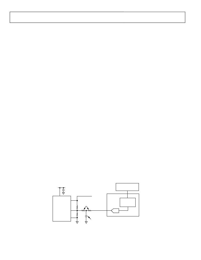
�OPEN-LOOP� SUPPLY� MARGINING�
�The� simplest� method� of� margining� a� supply� is� to� implement�
�an� open-loop� technique� (see� Figure� 32).� A� popular� way� to� do�
�this� is� to� switch� extra� resistors� into� the� feedback� node� of� a� power�
�module,� such� as� a� dc-to-dc� converter� or� LDO.� The� extra� resistor�
�alters� the� voltage� at� the� feedback� or� trim� node� and� forces� the�
�output� voltage� to� margin� up� or� down� by� a� certain� amount.�
�The� ADM1066� can� perform� open-loop� margining� for� up� to� six�
�supplies.� The� six� on-board� voltage� DACs� (DAC1� to� DAC6)�
�can� drive� into� the� feedback� pins� of� the� power� modules� to� be�
�margined.� The� simplest� circuit� to� implement� this� function� is�
�an� attenuation� resistor� that� connects� the� DACx� pin� to� the�
�feedback� node� of� a� dc-to-dc� converter.� When� the� DACx� output�
�voltage� is� set� equal� to� the� feedback� voltage,� no� current� flows�
�into� the� attenuation� resistor,� and� the� dc-to-dc� converter� output�
�voltage� does� not� change.� Taking� DACx� above� the� feedback�
�voltage� forces� current� into� the� feedback� node,� and� the� output� of�
�the� dc-to-dc� converter� is� forced� to� fall� to� compensate� for� this.�
�The� dc-to-dc� converter� output� can� be� forced� high� by� setting� the�
�DACx� output� voltage� lower� than� the� feedback� node� voltage.� The�
�series� resistor� can� be� split� in� two,� and� the� node� between� them�
�can� be� decoupled� with� a� capacitor� to� ground.� This� can� help� to�
�decouple� any� noise� picked� up� from� the� board.� Decoupling� to� a�
�ground� local� to� the� dc-to-dc� converter� is� recommended.�
�The� ADM1066� can� be� commanded� to� margin� a� supply� up� or�
�down� over� the� SMBus� by� updating� the� values� on� the� relevant�
�DAC� output.�
�VIN�
�V� OUT�
�CLOSED-LOOP� SUPPLY� MARGINING�
�A� more� accurate� and� comprehensive� method� of� margining� is� to�
�implement� a� closed-loop� system� (see� Figure� 33).� The� voltage� on�
�the� rail� to� be� margined� can� be� read� back� to� accurately� margin� the�
�rail� to� the� target� voltage.� The� ADM1066� incorporates� all� the� circuits�
�required� to� do� this,� with� the� 12-bit� successive� approximation�
�ADC� used� to� read� back� the� level� of� the� supervised� voltages,� and�
�the� six� voltage� output� DACs,� implemented� as� described� in� the�
��levels.� These� circuits� can� be� used� along� with� other� intelligence,�
�such� as� a� microcontroller,� to� implement� a� closed-loop� margining�
�system� that� allows� any� dc-to-dc� converter� or� LDO� supply� to� be�
�set� to� any� voltage,� accurate� to� within� ±0.5%� of� the� target.�
�To� implement� closed-loop� margining�
�1.� Disable� the� six� DACx� outputs.�
�2.� Set� the� DAC� output� voltage� equal� to� the� voltage� on� the�
�feedback� node.�
�3.� Enable� the� DAC.�
�4.� Read� the� voltage� at� the� dc-to-dc� converter� output� that� is�
�connected� to� one� of� the� VPx,� VH,� or� VXx� pins.�
�5.� If� necessary,� modify� the� DACx� output� code� up� or� down� to�
�adjust� the� dc-to-dc� converter� output� voltage.� Otherwise,�
�stop� because� the� target� voltage� has� been� reached.�
�6.� Set� the� DAC� output� voltage� to� a� value� that� alters� the� supply�
�output� by� the� required� amount� (for� example,� ±5%).�
�7.� Repeat� Step� 4� through� Step� 6� until� the� measured� supply�
�reaches� the� target� voltage.�
�Step� 1� to� Step� 3� ensure� that� when� the� DACx� output� buffer� is�
�turned� on,� it� has� little� effect� on� the� dc-to-dc� converter� output.�
�The� DAC� output� buffer� is� designed� to� power� up� without� glitching�
�by� first� powering� up� the� buffer� to� follow� the� pin� voltage.� It� does�
�not� drive� out� onto� the� pin� at� this� time.� Once� the� output� buffer� is�
�properly� enabled,� the� buffer� input� is� switched� over� to� the� DAC,�
�and� the� output� stage� of� the� buffer� is� turned� on.� Output� glitching�
�is� negligible.�
�MICROCONTROLLER�
�ADM1066�
�OUTPUT�
�DC-TO-DC�
�CONVERTER�
�FEEDBACK�
�R1�
�ATTENUATION�
�RESISTOR,� R3�
�DACx�
�DAC�
�DEVICE�
�CONTROLLER�
�(SMBus)�
�GND�
�R2�
�PCB�
�TRACE� NOISE�
�DECOUPLING�
�CAPACITOR�
�Figure� 32.� Open-Loop� Margining� System� Using� the� ADM1066�
�Rev.� E� |� Page� 22� of� 32�
�相关PDF资料 |
PDF描述 |
|---|---|
| ADM1067ACPZ | IC SEQUENCER/SUPERVISOR 40-LFCSP |
| ADM1068ASTZ-REEL7 | IC SEQUENCER/SUPERVISOR 32LQFP |
| ADM1069ACPZ-REEL7 | IC SUPERVISOR/SEQ PROG 40LFCSP |
| ADM1088AKS-REEL7 | IC SIMPLE SEQUENCER P-P SC70-6 |
| ADM1169ASTZ | IC SEQUENCER/SUPERVISOR 32LQFP |
相关代理商/技术参数 |
参数描述 |
|---|---|
| ADM1067 | 制造商:AD 制造商全称:Analog Devices 功能描述:Super Sequencer with Open-Loop Margining DACs |
| ADM1067ACP | 制造商:Analog Devices 功能描述:Sequencer 40-Pin LFCSP EP |
| ADM1067ACP-REEL | 制造商:Analog Devices 功能描述:Sequencer 40-Pin LFCSP EP T/R |
| ADM1067ACP-REEL7 | 制造商:Analog Devices 功能描述:Sequencer 40-Pin LFCSP EP T/R |
| ADM1067ACPZ | 功能描述:IC SEQUENCER/SUPERVISOR 40-LFCSP RoHS:是 类别:集成电路 (IC) >> PMIC - 监控器 系列:Super Sequencer® 标准包装:1 系列:- 类型:简单复位/加电复位 监视电压数目:1 输出:开路漏极或开路集电极 复位:高有效 复位超时:- 电压 - 阀值:1.8V 工作温度:-40°C ~ 125°C 安装类型:表面贴装 封装/外壳:6-TSOP(0.059",1.50mm 宽)5 引线 供应商设备封装:5-TSOP 包装:剪切带 (CT) 其它名称:NCP301HSN18T1GOSCT |
发布紧急采购,3分钟左右您将得到回复。