- 您现在的位置:买卖IC网 > PDF目录1775 > ADM1066ASUZ-REEL7 (Analog Devices Inc)IC SEQUENCER/SUPERVISOR 48TQFP PDF资料下载
参数资料
| 型号: | ADM1066ASUZ-REEL7 |
| 厂商: | Analog Devices Inc |
| 文件页数: | 9/32页 |
| 文件大小: | 0K |
| 描述: | IC SEQUENCER/SUPERVISOR 48TQFP |
| 标准包装: | 500 |
| 系列: | Super Sequencer® |
| 类型: | 序列发生器 |
| 监视电压数目: | 12 |
| 输出: | 可编程 |
| 电压 - 阀值: | 可调节/可选择 |
| 工作温度: | -40°C ~ 85°C |
| 安装类型: | 表面贴装 |
| 封装/外壳: | 48-TQFP |
| 供应商设备封装: | 48-TQFP(7x7) |
| 包装: | 带卷 (TR) |
| 配用: | EVAL-ADM1066TQEBZ-ND - BOARD EVALUATION FOR ADM1066TQ |
第1页第2页第3页第4页第5页第6页第7页第8页当前第9页第10页第11页第12页第13页第14页第15页第16页第17页第18页第19页第20页第21页第22页第23页第24页第25页第26页第27页第28页第29页第30页第31页第32页
�� ��
��
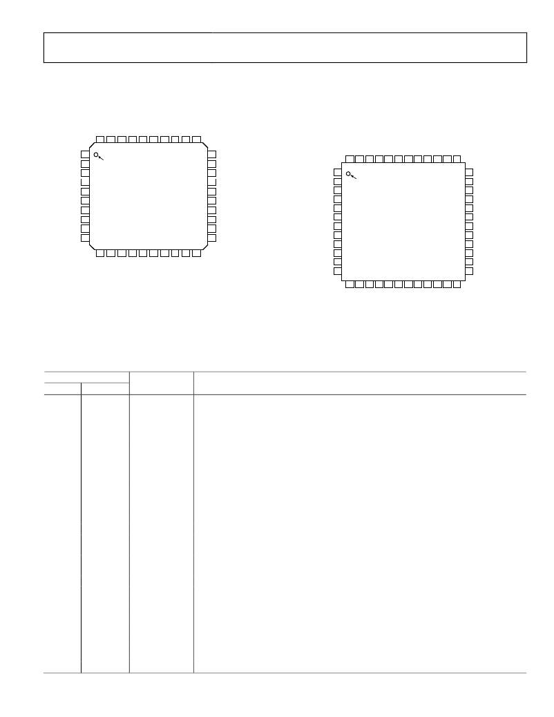
��ADM1066�
�PIN� CONFIGURATIONS� AND� FUNCTION� DESCRIPTIONS�
�40�
�39�
�38�
�37�
�36�
�35�
�34�
�33�
�32�
�31�
�VX1� 1�
�VX2� 2�
�PIN� 1�
�INDICATOR�
�30� PDO1�
�29� PDO2�
�48�
�47�
�46�
�45�
�44�
�43�
�42�
�41�
�40�
�39�
�38�
�37�
�VX3� 3�
�VX4� 4�
�VX5� 5�
�VP1� 6�
�VP2� 7�
�VP3� 8�
�VP4� 9�
�VH� 10�
�ADM1066�
�TOP� VIEW�
�(Not� to� Scale)�
�28� PDO3�
�27� PDO4�
�26� PDO5�
�25� PDO6�
�24� PDO7�
�23� PDO8�
�22� PDO9�
�21� PDO10�
�NC� 1�
�VX1� 2�
�VX2� 3�
�VX3� 4�
�VX4� 5�
�VX5� 6�
�VP1� 7�
�VP2� 8�
�VP3� 9�
�PIN� 1�
�INDICATOR�
�ADM1066�
�TOP� VIEW�
�(Not� to� Scale)�
�36� NC�
�35� PDO1�
�34� PDO2�
�33� PDO3�
�32� PDO4�
�31� PDO5�
�30� PDO6�
�29� PDO7�
�28� PDO8�
�11�
�12�
�13�
�14�
�15�
�16�
�17�
�18�
�19�
�20�
�VP4� 10�
�27� PDO9�
�VH� 11�
�NC� 12�
�26� PDO10�
�25� NC�
�NOTES�
�13�
�14�
�15�
�16�
�17�
�18�
�19�
�20�
�21�
�22�
�23�
�24�
�1.� NC� =� NO� CONNECT.�
�2.� THE� LFCSP� HAS� AN� EXPOSED� PAD� ON� THE� BOTTOM.�
�THIS� PAD� IS� A� NO� CONNECT� (NC).� IF� POSSIBLE,� THIS�
�PAD� SHOULD� BE� SOLDERED� TO� THE� BOARD� FOR�
�IMPROVED� MECHANICAL� STABILITY.�
�Figure� 3.� LFCSP� Pin� Configuration�
�Table� 4.� Pin� Function� Descriptions�
�Pin� No.�
�NC� =� NO� CONNECT�
�Figure� 4.� TQFP� Pin� Configuration�
�LFCSP�
�1�
�TQFP�
�1,� 12,� 13,�
�Mnemonic�
�NC�
�Description�
�No� Connection.�
�24,� 25,� 36,�
�37,� 48�
�1� to� 5�
�2� to� 6�
�VX1� to� VX5� (VXx)�
�High� Impedance� Inputs� to� Supply� Fault� Detectors.� Fault� thresholds� can� be� set� from� 0.573� V� to�
�1.375� V.� Alternatively,� these� pins� can� be� used� as� general-purpose� digital� inputs.�
�6� to� 9�
�7� to� 10�
�VP1� to� VP4� (VPx)�
�Low� Voltage� Inputs� to� Supply� Fault� Detectors.� Three� input� ranges� can� be� set� by� altering� the�
�input� attenuation� on� a� potential� divider� connected� to� these� pins,� the� output� of� which� connects�
�to� a� supply� fault� detector.� These� pins� allow� thresholds� from� 2.5� V� to� 6.0� V,� from� 1.25� V� to� 3.00� V,�
�and� from� 0.573� V� to� 1.375� V.�
�10�
�11�
�VH�
�High� Voltage� Input� to� Supply� Fault� Detectors.� Two� input� ranges� can� be� set� by� altering� the� input�
�attenuation� on� a� potential� divider� connected� to� this� pin,� the� output� of� which� connects� to� a�
�supply� fault� detector.� This� pin� allows� thresholds� from� 6.0� V� to� 14.4� V� and� from� 2.5� V� to� 6.0� V.�
�11�
�12�
�13�
�14�
�15�
�16�
�AGND� 2�
�REFGND� 2�
�REFIN�
�Ground� Return� for� Input� Attenuators.�
�Ground� Return� for� On-Chip� Reference� Circuits.�
�Reference� Input� for� ADC.� Nominally,� 2.048� V.� This� pin� must� be� driven� by� a� reference� voltage.�
�The� on-board� reference� can� be� used� by� connecting� the� REFOUT� pin� to� the� REFIN� pin.�
�14�
�17�
�REFOUT�
�Reference� Output,� 2.048� V.� Typically� connected� to� REFIN.� Note� that� the� capacitor� must� be�
�connected� between� this� pin� and� REFGND.� A� 10� μF� capacitor� is� recommended� for� this� purpose.�
�15� to� 20�
�21� to� 30�
�31�
�32�
�18� to� 23�
�26� to� 35�
�38�
�39�
�DAC1� to� DAC6�
�PDO10� to� PDO1�
�PDOGND� 2�
�VCCP�
�Voltage� Output� DACs.� These� pins� default� to� high� impedance� at� power-up.�
�Programmable� Driver� Outputs.�
�Ground� Return� for� Driver� Outputs.�
�Central� Charge-Pump� Voltage� of� 5.25� V.� A� reservoir� capacitor� must� be� connected� between� this�
�pin� and� GND.� A� 10� μF� capacitor� is� recommended� for� this� purpose.�
�33�
�34�
�35�
�36�
�40�
�41�
�42�
�43�
�A0�
�A1�
�SCL�
�SDA�
�Logic� Input.� This� pin� sets� the� seventh� bit� of� the� SMBus� interface� address.�
�Logic� Input.� This� pin� sets� the� sixth� bit� of� the� SMBus� interface� address.�
�SMBus� Clock� Pin.� Bidirectional,� open-drain� pin� that� requires� external� resistive� pull-up.�
�SMBus� Data� Pin.� Bidirectional,� open-drain� pin� that� requires� external� resistive� pull-up.�
�Rev.� E� |� Page� 9� of� 32�
�相关PDF资料 |
PDF描述 |
|---|---|
| ADM1067ACPZ | IC SEQUENCER/SUPERVISOR 40-LFCSP |
| ADM1068ASTZ-REEL7 | IC SEQUENCER/SUPERVISOR 32LQFP |
| ADM1069ACPZ-REEL7 | IC SUPERVISOR/SEQ PROG 40LFCSP |
| ADM1088AKS-REEL7 | IC SIMPLE SEQUENCER P-P SC70-6 |
| ADM1169ASTZ | IC SEQUENCER/SUPERVISOR 32LQFP |
相关代理商/技术参数 |
参数描述 |
|---|---|
| ADM1067 | 制造商:AD 制造商全称:Analog Devices 功能描述:Super Sequencer with Open-Loop Margining DACs |
| ADM1067ACP | 制造商:Analog Devices 功能描述:Sequencer 40-Pin LFCSP EP |
| ADM1067ACP-REEL | 制造商:Analog Devices 功能描述:Sequencer 40-Pin LFCSP EP T/R |
| ADM1067ACP-REEL7 | 制造商:Analog Devices 功能描述:Sequencer 40-Pin LFCSP EP T/R |
| ADM1067ACPZ | 功能描述:IC SEQUENCER/SUPERVISOR 40-LFCSP RoHS:是 类别:集成电路 (IC) >> PMIC - 监控器 系列:Super Sequencer® 标准包装:1 系列:- 类型:简单复位/加电复位 监视电压数目:1 输出:开路漏极或开路集电极 复位:高有效 复位超时:- 电压 - 阀值:1.8V 工作温度:-40°C ~ 125°C 安装类型:表面贴装 封装/外壳:6-TSOP(0.059",1.50mm 宽)5 引线 供应商设备封装:5-TSOP 包装:剪切带 (CT) 其它名称:NCP301HSN18T1GOSCT |
发布紧急采购,3分钟左右您将得到回复。