- 您现在的位置:买卖IC网 > PDF目录1775 > ADM1066ASUZ-REEL7 (Analog Devices Inc)IC SEQUENCER/SUPERVISOR 48TQFP PDF资料下载
参数资料
| 型号: | ADM1066ASUZ-REEL7 |
| 厂商: | Analog Devices Inc |
| 文件页数: | 26/32页 |
| 文件大小: | 0K |
| 描述: | IC SEQUENCER/SUPERVISOR 48TQFP |
| 标准包装: | 500 |
| 系列: | Super Sequencer® |
| 类型: | 序列发生器 |
| 监视电压数目: | 12 |
| 输出: | 可编程 |
| 电压 - 阀值: | 可调节/可选择 |
| 工作温度: | -40°C ~ 85°C |
| 安装类型: | 表面贴装 |
| 封装/外壳: | 48-TQFP |
| 供应商设备封装: | 48-TQFP(7x7) |
| 包装: | 带卷 (TR) |
| 配用: | EVAL-ADM1066TQEBZ-ND - BOARD EVALUATION FOR ADM1066TQ |
第1页第2页第3页第4页第5页第6页第7页第8页第9页第10页第11页第12页第13页第14页第15页第16页第17页第18页第19页第20页第21页第22页第23页第24页第25页当前第26页第27页第28页第29页第30页第31页第32页
�� �
�
�ADM1066�
�SMBus�
�POWER-UP�
�(V� CC� >� 2.5V)�
�EEPROM�
�E�
�E�
�P�
�R�
�O�
�M�
�L�
�D�
�DEVICE�
�CONTROLLER�
�D�
�A�
�T�
�A�
�LATCH� A�
�R�
�A�
�M�
�L�
�D�
�U�
�P�
�D�
�LATCH� B�
�FUNCTION�
�(OV� THRESHOLD�
�ON� VP1)�
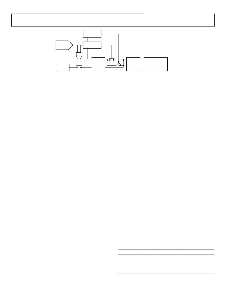
�Figure� 35.� Configuration� Update� Flow� Diagram�
�UPDATING� THE� SEQUENCING� ENGINE�
�Sequencing� engine� (SE)� functions� are� not� updated� in� the� same�
�The� major� differences� between� the� EEPROM� and� other�
�registers� are� as� follows:�
�way� as� regular� configuration� latches.� The� SE� has� its� own� dedicated�
�512-byte� nonvolatile,� electrically� erasable,� programmable,� read-�
�only� memory� (EEPROM)� for� storing� state� definitions,� providing�
�63� individual� states� each� with� a� 64-bit� word� (one� state� is� reserved).�
�?�
�?�
�?�
�An� EEPROM� location� must� be� blank� before� it� can� be�
�written� to.� If� it� contains� data,� the� data� must� first� be� erased.�
�Writing� to� the� EEPROM� is� slower� than� writing� to� the� RAM.�
�Writing� to� the� EEPROM� should� be� restricted� because� it� has�
�At� power-up,� the� first� state� is� loaded� from� the� SE� EEPROM� into�
�the� engine� itself.� When� the� conditions� of� this� state� are� met,� the�
�next� state� is� loaded� from� the� EEPROM� into� the� engine,� and� so�
�on.� The� loading� of� each� new� state� takes� approximately� 10� μs.�
�To� alter� a� state,� the� required� changes� must� be� made� directly� to�
�the� EEPROM.� RAM� for� each� state� does� not� exist.� The� relevant�
�alterations� must� be� made� to� the� 64-bit� word,� which� is� then�
�uploaded� directly� to� the� EEPROM.�
�INTERNAL� REGISTERS�
�The� ADM1066� contains� a� large� number� of� data� registers.� The�
�a� limited� write/cycle� life� of� typically� 10,000� write� operations�
�due� to� the� usual� EEPROM� wear-out� mechanisms.�
�The� first� EEPROM� is� split� into� 16� (0� to� 15)� pages� of� 32� bytes�
�each.� Page� 0� to� Page� 6,� starting� at� Address� 0xF800,� hold� the�
�configuration� data� for� the� applications� on� the� ADM1066� (such�
�as� the� SFDs� and� PDOs).� These� EEPROM� addresses� are� the� same�
�as� the� RAM� register� addresses,� prefixed� by� F8.� Page� 7� is�
�reserved.� Page� 8� to� Page� 15� are� for� customer� use.�
�Data� can� be� downloaded� from� the� EEPROM� to� the� RAM� in� one�
�of� the� following� ways:�
�principal� registers� are� the� address� pointer� register� and� the�
�configuration� registers.�
�?�
�?�
�At� power-up,� when� Page� 0� to� Page� 6� are� downloaded�
�By� setting� Bit� 0� of� the� UDOWNLD� register� (0xD8),� which�
�Address� Pointer� Register�
�The� address� pointer� register� contains� the� address� that� selects�
�one� of� the� other� internal� registers.� When� writing� to� the� ADM1066,�
�the� first� byte� of� data� is� always� a� register� address� that� is� written�
�to� the� address� pointer� register.�
�Configuration� Registers�
�The� configuration� registers� provide� control� and� configuration�
�for� various� operating� parameters� of� the� ADM1066.�
�EEPROM�
�The� ADM1066� has� two� 512-byte� cells� of� nonvolatile� EEPROM�
�from� Register� Address� 0xF800� to� Register� Address� 0xFBFF.� The�
�EEPROM� is� used� for� permanent� storage� of� data� that� is� not� lost�
�when� the� ADM1066� is� powered� down.� One� EEPROM� cell� contains�
�the� configuration� data� of� the� device;� the� other� contains� the� state�
�performs� a� user� download� of� Page� 0� to� Page� 6�
�SERIAL� BUS� INTERFACE�
�The� ADM1066� is� controlled� via� the� serial� system� management�
�bus� (SMBus)� and� is� connected� to� this� bus� as� a� slave� device� under�
�the� control� of� a� master� device.� It� takes� approximately� 1� ms� after�
�power-up� for� the� ADM1066� to� download� from� its� EEPROM.�
�Therefore,� access� to� the� ADM1066� is� restricted� until� the�
�download� is� complete.�
�Identifying� the� ADM1066� on� the� SMBus�
�The� ADM1066� has� a� 7-bit� serial� bus� slave� address� (see� Table� 11).�
�The� device� is� powered� up� with� a� default� serial� bus� address.� The�
�five� MSBs� of� the� address� are� set� to� 01101;� the� two� LSBs� are�
�determined� by� the� logical� states� of� Pin� A1� and� Pin� A0.� This�
�allows� the� connection� of� four� ADM1066s� to� one� SMBus.�
�definitions� for� the� SE.� Although� referred� to� as� read-only� memory,�
�the� EEPROM� can� be� written� to,� as� well� as� read� from,� using� the�
�serial� bus� in� exactly� the� same� way� as� the� other� registers.�
�Table� 11.� Serial� Bus� Slave� Address�
�A1� Pin� A0� Pin� Hex� Address�
�Low� Low� 0x68�
�7-Bit� Address�
�0110100x� 1�
�Low�
�High�
�High�
�High�
�Low�
�High�
�0x6A�
�0x6C�
�0x6E�
�0110101x� 1�
�0110110x� 1�
�0110111x� 1�
�1�
�x� =� Read/write� bit.� The� address� is� shown� only� as� the� first� 7� MSBs.�
�Rev.� E� |� Page� 26� of� 32�
�相关PDF资料 |
PDF描述 |
|---|---|
| ADM1067ACPZ | IC SEQUENCER/SUPERVISOR 40-LFCSP |
| ADM1068ASTZ-REEL7 | IC SEQUENCER/SUPERVISOR 32LQFP |
| ADM1069ACPZ-REEL7 | IC SUPERVISOR/SEQ PROG 40LFCSP |
| ADM1088AKS-REEL7 | IC SIMPLE SEQUENCER P-P SC70-6 |
| ADM1169ASTZ | IC SEQUENCER/SUPERVISOR 32LQFP |
相关代理商/技术参数 |
参数描述 |
|---|---|
| ADM1067 | 制造商:AD 制造商全称:Analog Devices 功能描述:Super Sequencer with Open-Loop Margining DACs |
| ADM1067ACP | 制造商:Analog Devices 功能描述:Sequencer 40-Pin LFCSP EP |
| ADM1067ACP-REEL | 制造商:Analog Devices 功能描述:Sequencer 40-Pin LFCSP EP T/R |
| ADM1067ACP-REEL7 | 制造商:Analog Devices 功能描述:Sequencer 40-Pin LFCSP EP T/R |
| ADM1067ACPZ | 功能描述:IC SEQUENCER/SUPERVISOR 40-LFCSP RoHS:是 类别:集成电路 (IC) >> PMIC - 监控器 系列:Super Sequencer® 标准包装:1 系列:- 类型:简单复位/加电复位 监视电压数目:1 输出:开路漏极或开路集电极 复位:高有效 复位超时:- 电压 - 阀值:1.8V 工作温度:-40°C ~ 125°C 安装类型:表面贴装 封装/外壳:6-TSOP(0.059",1.50mm 宽)5 引线 供应商设备封装:5-TSOP 包装:剪切带 (CT) 其它名称:NCP301HSN18T1GOSCT |
发布紧急采购,3分钟左右您将得到回复。