- 您现在的位置:买卖IC网 > PDF目录1775 > ADM1066ASUZ-REEL7 (Analog Devices Inc)IC SEQUENCER/SUPERVISOR 48TQFP PDF资料下载
参数资料
| 型号: | ADM1066ASUZ-REEL7 |
| 厂商: | Analog Devices Inc |
| 文件页数: | 30/32页 |
| 文件大小: | 0K |
| 描述: | IC SEQUENCER/SUPERVISOR 48TQFP |
| 标准包装: | 500 |
| 系列: | Super Sequencer® |
| 类型: | 序列发生器 |
| 监视电压数目: | 12 |
| 输出: | 可编程 |
| 电压 - 阀值: | 可调节/可选择 |
| 工作温度: | -40°C ~ 85°C |
| 安装类型: | 表面贴装 |
| 封装/外壳: | 48-TQFP |
| 供应商设备封装: | 48-TQFP(7x7) |
| 包装: | 带卷 (TR) |
| 配用: | EVAL-ADM1066TQEBZ-ND - BOARD EVALUATION FOR ADM1066TQ |
第1页第2页第3页第4页第5页第6页第7页第8页第9页第10页第11页第12页第13页第14页第15页第16页第17页第18页第19页第20页第21页第22页第23页第24页第25页第26页第27页第28页第29页当前第30页第31页第32页
�� �
�
�ADM1066�
�Unlike� some� EEPROM� devices� that� limit� block� writes� to� within�
�a� page� boundary,� there� is� no� limitation� on� the� start� address�
�when� performing� a� block� write� to� EEPROM,� except� when�
�5.�
�6.�
�7.�
�The� slave� asserts� an� ACK� on� SDA.�
�The� master� asserts� a� repeat� start� condition� on� SDA.�
�The� master� sends� the� 7-bit� slave� address� followed� by� the�
�?�
�?�
�There� must� be� at� least� N� locations� from� the� start� address� to�
�the� highest� EEPROM� address� (0xFBFF)� to� avoid� writing� to�
�invalid� addresses.�
�An� address� crosses� a� page� boundary.� In� this� case,� both�
�pages� must� be� erased� before� programming.�
�8.�
�9.�
�read� bit� (high).�
�The� slave� asserts� an� ACK� on� SDA.�
�The� ADM1066� sends� a� byte-count� data� byte� that� tells� the�
�master� how� many� data� bytes� to� expect.� The� ADM1066�
�always� returns� 32� data� bytes� (0x20),� which� is� the� maximum�
�allowed� by� the� SMBus� Version� 1.1� specification.�
�Note� that� the� ADM1066� features� a� clock� extend� function� for� writes�
�to� the� EEPROM.� Programming� an� EEPROM� byte� takes� approxi-�
�mately� 250� μs,� which� limits� the� SMBus� clock� for� repeated� or� block�
�write� operations.� The� ADM1066� pulls� SCL� low� and� extends� the�
�clock� pulse� when� it� cannot� accept� any� more� data.�
�10.�
�11.�
�12.�
�13.�
�The� master� asserts� an� ACK� on� SDA.�
�The� master� receives� 32� data� bytes.�
�The� master� asserts� an� ACK� on� SDA� after� each� data� byte.�
�The� master� asserts� a� stop� condition� on� SDA� to� end� the�
�transaction.�
�READ� OPERATIONS�
�The� ADM1066� uses� the� following� SMBus� read� protocols.�
�1�
�S�
�2�
�SLAVE�
�ADDRESS�
�3�
�W� A�
�4�
�COMMAND� 0xFD�
�(BLOCK� READ)�
�5� 6�
�A� S�
�7�
�SLAVE�
�ADDRESS�
�8�
�R� A�
�9�
�BYTE�
�COUNT�
�10�
�A�
�11�
�DATA�
�1�
�12�
�A�
�Receive� Byte�
�In� a� receive� byte� operation,� the� master� device� receives� a� single�
�13�
�byte� from� a� slave� device,� as� follows:�
�DATA�
�32�
�A�
�P�
�1.�
�2.�
�3.�
�4.�
�5.�
�6.�
�The� master� device� asserts� a� start� condition� on� SDA.�
�The� master� sends� the� 7-bit� slave� address� followed� by� the�
�read� bit� (high).�
�The� addressed� slave� device� asserts� an� ACK� on� SDA.�
�The� master� receives� a� data� byte.�
�The� master� asserts� a� NACK� on� SDA.�
�The� master� asserts� a� stop� condition� on� SDA,� and� the�
�Figure� 46.� Block� Read� from� the� EEPROM� or� RAM�
�Error� Correction�
�The� ADM1066� provides� the� option� of� issuing� a� packet� error� correc-�
�tion� (PEC)� byte� after� a� write� to� the� RAM,� a� write� to� the� EEPROM,�
�a� block� write� to� the� RAM/EEPROM,� or� a� block� read� from� the�
�RAM/EEPROM.� This� option� enables� the� user� to� verify� that� the� data�
�transaction� ends.�
�In� the� ADM1066,� the� receive� byte� protocol� is� used� to� read� a�
�single� byte� of� data� from� a� RAM� or� EEPROM� location� whose�
�address� has� previously� been� set� by� a� send� byte� or� write�
��1� 2� 3� 4� 5� 6�
�received� by� or� sent� from� the� ADM1066� is� correct.� The� PEC� byte�
�is� an� optional� byte� sent� after� the� last� data� byte� has� been� written�
�to� or� read� from� the� ADM1066.� The� protocol� is� the� same� as� a�
�block� read� for� Step� 1� to� Step� 12� and� then� proceeds� as� follows:�
�13.� The� ADM1066� issues� a� PEC� byte� to� the� master.� The� master�
�checks� the� PEC� byte� and� issues� another� block� read,� if� the�
�PEC� byte� is� incorrect.�
�S�
�SLAVE�
�ADDRESS�
�R�
�A�
�DATA�
�A�
�P�
�14.� A� NACK� is� generated� after� the� PEC� byte� to� signal� the� end�
�of� the� read.�
�Figure� 45.� Single� Byte� Read� from� the� EEPROM� or� RAM�
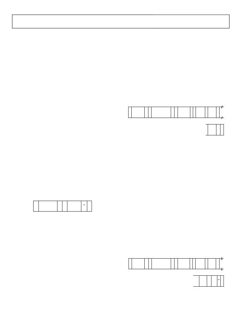
�Block� Read�
�In� a� block� read� operation,� the� master� device� reads� a� block� of�
�data� from� a� slave� device.� The� start� address� for� a� block� read� must�
�have� been� set� previously.� In� the� ADM1066,� this� is� done� by� a�
�send� byte� operation� to� set� a� RAM� address,� or� a� write� byte/word�
�operation� to� set� an� EEPROM� address.� The� block� read� operation�
�itself� consists� of� a� send� byte� operation� that� sends� a� block� read�
�15.� The� master� asserts� a� stop� condition� on� SDA� to� end� the�
�transaction.�
�Note� that� the� PEC� byte� is� calculated� using� CRC-8.� The� frame�
�check� sequence� (FCS)� conforms� to� CRC-8� by� the� polynomial�
�C� (� x� )� =� x� 8� +� x� 2� +� x� 1� +� 1�
�See� the� SMBus� Version� 1.1� specification� for� details.� An� example�
��command� to� the� slave,� immediately� followed� by� a� repeated� start�
�1�
�2�
�3�
�4�
�5� 6�
�7�
�8�
�9�
�10�
�11�
�12�
�W� A� COMMAND� 0xFD� A� S�
�BYTE� A� DATA� A�
�and� a� read� operation� that� reads� out� multiple� data� bytes,� as� follows:�
�S�
�SLAVE�
�ADDRESS�
�(BLOCK� READ)�
�SLAVE�
�ADDRESS�
�R� A�
�COUNT� 1�
�1.�
�The� master� device� asserts� a� start� condition� on� SDA.�
�2.�
�The� master� sends� the� 7-bit� slave� address� followed� by� the�
�13� 14� 15�
�3.�
�write� bit� (low).�
�The� addressed� slave� device� asserts� an� ACK� on� SDA.�
�DATA�
�32�
�A� PEC� A� P�
�4.�
�The� master� sends� a� command� code� that� tells� the� slave�
�device� to� expect� a� block� read.� The� ADM1066� command�
�code� for� a� block� read� is� 0xFD� (1111� 1101).�
�Rev.� E� |� Page� 30� of� 32�
�Figure� 47.� Block� Read� from� the� EEPROM� or� RAM� with� PEC�
�相关PDF资料 |
PDF描述 |
|---|---|
| ADM1067ACPZ | IC SEQUENCER/SUPERVISOR 40-LFCSP |
| ADM1068ASTZ-REEL7 | IC SEQUENCER/SUPERVISOR 32LQFP |
| ADM1069ACPZ-REEL7 | IC SUPERVISOR/SEQ PROG 40LFCSP |
| ADM1088AKS-REEL7 | IC SIMPLE SEQUENCER P-P SC70-6 |
| ADM1169ASTZ | IC SEQUENCER/SUPERVISOR 32LQFP |
相关代理商/技术参数 |
参数描述 |
|---|---|
| ADM1067 | 制造商:AD 制造商全称:Analog Devices 功能描述:Super Sequencer with Open-Loop Margining DACs |
| ADM1067ACP | 制造商:Analog Devices 功能描述:Sequencer 40-Pin LFCSP EP |
| ADM1067ACP-REEL | 制造商:Analog Devices 功能描述:Sequencer 40-Pin LFCSP EP T/R |
| ADM1067ACP-REEL7 | 制造商:Analog Devices 功能描述:Sequencer 40-Pin LFCSP EP T/R |
| ADM1067ACPZ | 功能描述:IC SEQUENCER/SUPERVISOR 40-LFCSP RoHS:是 类别:集成电路 (IC) >> PMIC - 监控器 系列:Super Sequencer® 标准包装:1 系列:- 类型:简单复位/加电复位 监视电压数目:1 输出:开路漏极或开路集电极 复位:高有效 复位超时:- 电压 - 阀值:1.8V 工作温度:-40°C ~ 125°C 安装类型:表面贴装 封装/外壳:6-TSOP(0.059",1.50mm 宽)5 引线 供应商设备封装:5-TSOP 包装:剪切带 (CT) 其它名称:NCP301HSN18T1GOSCT |
发布紧急采购,3分钟左右您将得到回复。