- 您现在的位置:买卖IC网 > PDF目录1776 > ADN2530YCPZ-500R7 (Analog Devices Inc)IC LASER DRVR 11.3GPBS 16LFCSP PDF资料下载
参数资料
| 型号: | ADN2530YCPZ-500R7 |
| 厂商: | Analog Devices Inc |
| 文件页数: | 13/20页 |
| 文件大小: | 0K |
| 描述: | IC LASER DRVR 11.3GPBS 16LFCSP |
| 标准包装: | 1 |
| 类型: | 激光二极管驱动器(光纤) |
| 数据速率: | 11.3Gbps |
| 通道数: | 1 |
| 电源电压: | 3.07 V ~ 3.53 V |
| 电流 - 电源: | 27mA |
| 电流 - 调制: | 23mA |
| 电流 - 偏置: | 25mA |
| 工作温度: | -40°C ~ 100°C |
| 封装/外壳: | 16-VFQFN 裸露焊盘,CSP |
| 供应商设备封装: | 16-LFCSP-VQ |
| 包装: | 标准包装 |
| 安装类型: | 表面贴装 |
| 其它名称: | ADN2530YCPZ-500R7DKR |
�� �
�
�P� =� VCC� � ?� MSET� +� I� SUPPLY� ?� +� V� IBIAS� � (� IBIAS� � 1� .� 2� )�
�P� =� VCC� � ?� MSET� +� I� SUPPLY� ?� +� V� IBIAS� � ?� BSET� � 1� .� 2� ?�
�DataSheet�
�LOAD� MISTERMINATION�
�Due� to� its� excellent� S22� performance,� the� ADN2530� can� drive�
�differential� loads� that� range� from� 35� ?� to� 140� ?.� In� practice,�
�many� TOSAs� have� differential� resistance� not� equal� to� 100� ?.� In�
�this� case,� with� 100� ?� differential� transmission� lines� connecting�
�the� ADN2530� to� the� load,� the� load� end� of� the� transmission� lines�
�are� misterminated.� This� mistermination� leads� to� signal� reflections�
�back� to� the� driver.� The� excellent� back-termination� in� the�
�ADN2530� absorbs� these� reflections,� preventing� their� reflection�
�back� to� the� load.� This� enables� excellent� optical� eye� quality� to�
�be� achieved� even� when� the� load� end� of� the� transmission� lines� is�
�significantly� misterminated.� The� connection� between� the� load�
�and� the� ADN2530� must� be� made� with� 100� ?� differential� (50� ?�
�single-ended)� transmission� lines� so� that� the� driver� end� of� the�
�transmission� lines� is� properly� terminated.�
�CROSSPOINT� ADJUST�
�The� crossing� level� in� the� output� electrical� eye� diagram� can� be�
�adjusted� between� 35%� and� 65%� using� the� crosspoint� adjust� (CPA)�
�control� input.� This� can� be� used� to� compensate� for� asymmetry� in�
�the� VCSEL� response� and� optimizes� the� optical� eye� mask� margin.�
�The� CPA� input� is� a� voltage� control� input,� and� a� plot� of� eye� cross-�
��in� the� Typical� Performance� Characteristics� section.� The� equivalent�
�circuit� for� the� CPA� pin� is� shown� in� Figure� 36.� To� disable� the�
�ADN2530�
�POWER� CONSUMPTION�
�The� power� dissipated� by� the� ADN2530� is� given� by�
�?� V� ?�
�?� 50� ?�
�where:�
�VCC� is� the� power� supply� voltage.�
��V� MSET� is� the� voltage� applied� to� the� MSET� pin.�
�I� SUPPLY� is� the� sum� of� the� current� that� flows� into� the� VCC,�
�IMODP,� and� IMODN� pins� of� the� ADN2530� when� IBIAS� =�
��V� IBIAS� is� the� average� voltage� on� the� IBIAS� pin.�
�Considering� VBSET/IBIAS� =� 50� as� the� conversion� factor� from�
�V� BSET� to� IBIAS,� the� dissipated� power� becomes�
�?� V� ?� ?� V� ?�
�?� 50� ?� ?� 50� ?�
�To� ensure� long-term� reliable� operation,� the� junction� tempera-�
�ture� of� the� ADN2530� must� not� exceed� 125°C,� as� specified� in�
���crosspoint� adjust� function� and� set� the� eye� crossing� to� 50%,� the�
�CPA� pin� should� be� tied� to� VCC.�
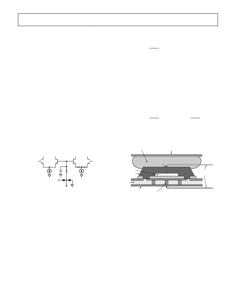
�THERMAL� COMPOUND�
�MODULE� CASE�
�T� TOP�
�100� ?�
�DIE�
�T� J�
�THERMO-COUPLE�
�PACKAGE�
�T� PAD�
�VCC�
�PCB�
�CPA�
�COPPER� PLANE�
�Figure� 36.� Equivalent� Circuit� for� CPA� Pin�
�Rev.� B� |� Page� 13� of� 20�
�VIAS�
�Figure� 37.� Typical� Optical� Module� Structure�
�相关PDF资料 |
PDF描述 |
|---|---|
| ADN2531ACPZ-R2 | IC LASER DRIVER 11.3GBPS 16LFCSP |
| ADN2830ACPZ32 | IC LASR CTRLR 1CHAN 5.5V 32LFCSP |
| ADN2841ACPZ-48 | IC LSR DRVR 2.7GBPS 5.5V 48LFCSP |
| ADN2847ACPZ-32 | IC LSR DRVR 3.3GBPS 3.6V 32LFCSP |
| ADN2848ACPZ-32-RL7 | IC LASER DRIVER 1.25GBPS 32LFCSP |
相关代理商/技术参数 |
参数描述 |
|---|---|
| ADN2530YCPZ-R2 | 制造商:AD 制造商全称:Analog Devices 功能描述:11.3 Gbps, Active Back-Termination, Differential VCSEL Driver |
| adn2530ycpz-reel7 | 制造商:Analog Devices 功能描述:LASER DRVR VCSEL 11.3GBPS 1CH 16LFCSP - Tape and Reel 制造商:Rochester Electronics LLC 功能描述: |
| ADN2530YCPZ-WP | 制造商:Analog Devices 功能描述:LASER DRVR VCSEL 11.3GBPS 1CH 16LFCSP - Waffle Pack |
| ADN2531 | 制造商:AD 制造商全称:Analog Devices 功能描述:11.3 Gbps, Active Back-Termination, Differential Laser Diode Driver |
| ADN2531ACPZ | 制造商:Analog Devices 功能描述: |
发布紧急采购,3分钟左右您将得到回复。