- 您现在的位置:买卖IC网 > PDF目录9375 > ADN2850BCPZ250 (Analog Devices Inc)IC DGTL RHEO DL 1024POS 16LFCSP PDF资料下载
参数资料
| 型号: | ADN2850BCPZ250 |
| 厂商: | Analog Devices Inc |
| 文件页数: | 11/28页 |
| 文件大小: | 0K |
| 描述: | IC DGTL RHEO DL 1024POS 16LFCSP |
| 产品变化通告: | Metal Edit Change 03/Feb/2012 |
| 标准包装: | 1 |
| 接片: | 1024 |
| 电阻(欧姆): | 250k |
| 电路数: | 2 |
| 温度系数: | 标准值 35 ppm/°C |
| 存储器类型: | 非易失 |
| 接口: | 4 线 SPI(芯片选择) |
| 电源电压: | 3 V ~ 5.5 V,±2.25 V ~ 2.75 V |
| 工作温度: | -40°C ~ 85°C |
| 安装类型: | 表面贴装 |
| 封装/外壳: | 16-VQFN 裸露焊盘,CSP |
| 供应商设备封装: | 16-LFCSP |
| 包装: | 托盘 |
第1页第2页第3页第4页第5页第6页第7页第8页第9页第10页当前第11页第12页第13页第14页第15页第16页第17页第18页第19页第20页第21页第22页第23页第24页第25页第26页第27页第28页
Data Sheet
ADN2850
Rev. E | Page 19 of 28
PROGRAMMING THE VARIABLE RESISTOR
The nominal resistance of the RDAC between Terminal W and
Terminal B, RWB, is available with 25 k and 250 k with
1024 positions (10-bit resolution). The final digits of the part
number determine the nominal resistance value, for example,
25 k = 24.4 ; 250 k = 244 .
The 10-bit data-word in the RDAC latch is decoded to select one of
the 1024 possible settings. The following description provides the
calculation of resistance, RWB, at different codes of a 25 k part.
The first connection of the wiper starts at Terminal B for
Data 0x000. RWB(0) is 30 because of the wiper resistance, and
it is independent of the nominal resistance. The second connection
is the first tap point where RWB(1) becomes 24.4 + 30 = 54.4
for Data 0x001. The third connection is the next tap point
representing RWB(2) = 48.8 + 30 = 78.8 for Data 0x002,
and so on. Each LSB data value increase moves the wiper up the
resistor ladder until the last tap point is reached at RWB(1023) =
25006 . See Figure 32 for a simplified diagram of the equivalent
RDAC circuit.
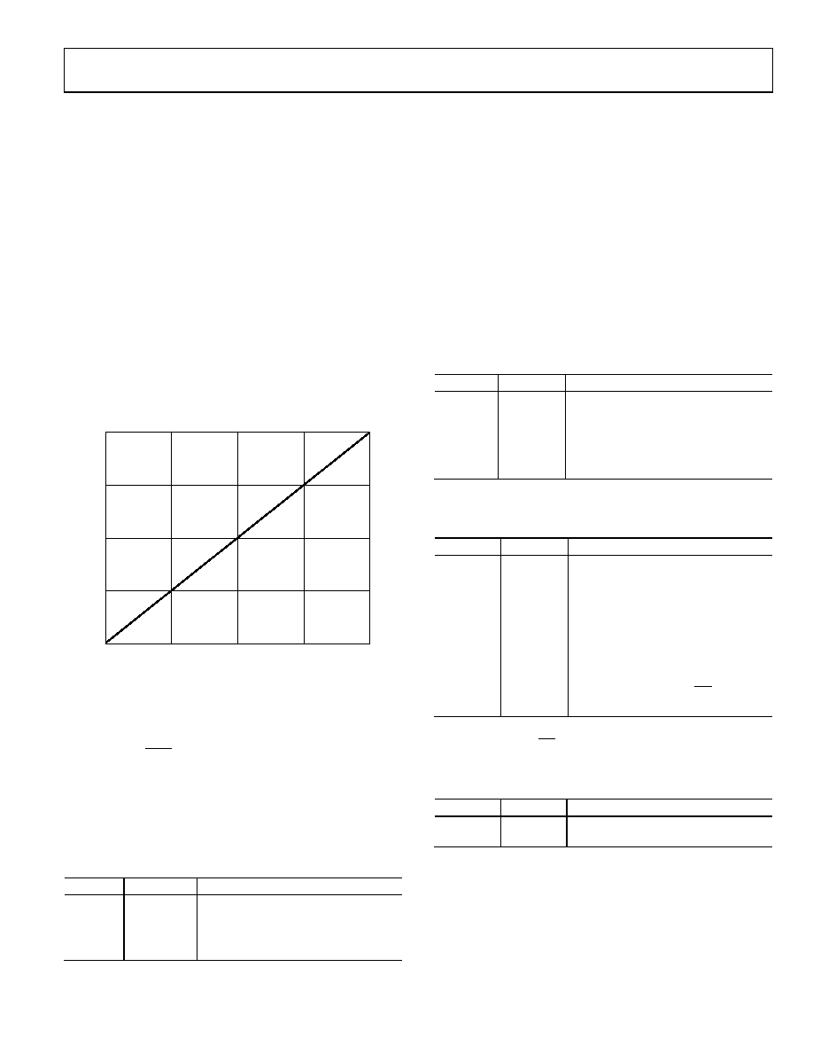
CODE (Decimal)
100
75
0
1023
256
R
W
B
(D
)
(%
R
W
F
)
512
768
50
25
RWB
0
2
6
0
-0
4
5
Figure 33. RWB(D) vs. Decimal Code
The general equation that determines the programmed output
resistance between Terminal Bx and Terminal Wx is
W
NOM
WB
R
D
R
+
×
=
_
1024
)
(
(1)
where:
D is the decimal equivalent of the data contained in the RDAC
register.
RWB_NOM is the nominal resistance value
RW is the wiper resistance.
Table 13. RWB (D) at Selected Codes for RWB_NOM = 25 k
D (Dec)
RWB(D) ()
Output State
1023
25,006
Full scale
512
12,530
Midscale
1
54.4
1 LSB
0
30
Zero scale (wiper contact resistor)
Note that, in the zero-scale condition, a finite wiper resistance
of 30 is present. Care should be taken to limit the current
flow between W and B in this state to no more than 20 mA to
avoid degradation or possible destruction of the internal switches.
The typical distribution of RWB_NOM from channel to channel is
±0.2% within the same package. Device-to-device matching is
process lot dependent upon the worst case of ±30% variation.
However, the change in RWBat full scale with temperature has a
35 ppm/°C temperature coefficient.
PROGRAMMING EXAMPLES
The following programming examples illustrate a typical sequence
of events for various features of the ADN2850. See Table 8 for
the instructions and data-word format. The instruction numbers,
addresses, and data appearing at the SDI and SDO pins are in
hexadecimal format.
Table 14. Scratchpad Programming
SDI
SDO
Action
0xB00100
0xXXXXXX
Writes Data 0x100 into RDAC1 register,
Wiper W1 moves to 1/4 full-scale
position.
0xB10200
0xB00100
Loads Data 0x200 into RDAC2 register,
Wiper W2 moves to 1/2 full-scale
position.
Table 15. Incrementing RDAC Followed by Storing the
Wiper Setting to EEMEM
SDI
SDO
Action
0xB00100
0xXXXXXX
Writes Data 0x100 into RDAC1
register, Wiper W1 moves to 1/4 full-
scale position.
0xE0XXXX
0xB00100
Increments RDAC1 register by one to
0x101.
0xE0XXXX
Increments RDAC1 register by one to
0x102. Continue until desired wiper
position is reached.
0x20XXXX
0xXXXXXX
Stores RDAC2 register data into
EEMEM1. Optionally, tie
AA
WPEE
AA
to GND to
protect EEMEM values.
The EEMEM values for the RDACs can be restored by power-
on, by strobing the
AA
PREE
AA
pin, or by the two commands shown in
Table 16. Restoring the EEMEM Values to RDAC Registers
SDI
SDO
Action
0x10XXXX
0xXXXXXX
Restores the EEMEM1 value to the
RDAC1 register.
相关PDF资料 |
PDF描述 |
|---|---|
| VE-B3J-MY-F4 | CONVERTER MOD DC/DC 36V 50W |
| AD5232BRU10 | IC DGTL POT 256POS 10K 16TSSOP |
| VI-2NW-MX-B1 | CONVERTER MOD DC/DC 5.5V 75W |
| VE-B3J-MY-F3 | CONVERTER MOD DC/DC 36V 50W |
| AD8403ARZ50 | IC DCP QUAD 50K 24-SOIC |
相关代理商/技术参数 |
参数描述 |
|---|---|
| ADN2850BCPZ250-RL7 | 功能描述:IC DGTL RHEO DL 25K 9BIT16LFCSP RoHS:是 类别:集成电路 (IC) >> 数据采集 - 数字电位器 系列:- 标准包装:3,000 系列:DPP 接片:32 电阻(欧姆):10k 电路数:1 温度系数:标准值 300 ppm/°C 存储器类型:非易失 接口:3 线串行(芯片选择,递增,增/减) 电源电压:2.5 V ~ 6 V 工作温度:-40°C ~ 85°C 安装类型:表面贴装 封装/外壳:8-WFDFN 裸露焊盘 供应商设备封装:8-TDFN(2x3) 包装:带卷 (TR) |
| ADN2850BCPZ25-RL7 | 功能描述:IC DGTL RHEO DL 25K 9BIT16LFCSP RoHS:是 类别:集成电路 (IC) >> 数据采集 - 数字电位器 系列:- 标准包装:3,000 系列:DPP 接片:32 电阻(欧姆):10k 电路数:1 温度系数:标准值 300 ppm/°C 存储器类型:非易失 接口:3 线串行(芯片选择,递增,增/减) 电源电压:2.5 V ~ 6 V 工作温度:-40°C ~ 85°C 安装类型:表面贴装 封装/外壳:8-WFDFN 裸露焊盘 供应商设备封装:8-TDFN(2x3) 包装:带卷 (TR) |
| ADN2850BRU25 | 制造商:Analog Devices 功能描述: |
| adn2850bru25-rl7 | 制造商:Analog Devices 功能描述: |
| ADN2850BRUZ25 | 制造商:Analog Devices 功能描述:DUAL 9-BIT SPI DIG. POT - Rail/Tube 制造商:Analog Devices 功能描述:Dual 10-B Progable Non-Volatile Resistor |
发布紧急采购,3分钟左右您将得到回复。