- 您现在的位置:买卖IC网 > PDF目录9375 > ADN2850BCPZ250 (Analog Devices Inc)IC DGTL RHEO DL 1024POS 16LFCSP PDF资料下载
参数资料
| 型号: | ADN2850BCPZ250 |
| 厂商: | Analog Devices Inc |
| 文件页数: | 6/28页 |
| 文件大小: | 0K |
| 描述: | IC DGTL RHEO DL 1024POS 16LFCSP |
| 产品变化通告: | Metal Edit Change 03/Feb/2012 |
| 标准包装: | 1 |
| 接片: | 1024 |
| 电阻(欧姆): | 250k |
| 电路数: | 2 |
| 温度系数: | 标准值 35 ppm/°C |
| 存储器类型: | 非易失 |
| 接口: | 4 线 SPI(芯片选择) |
| 电源电压: | 3 V ~ 5.5 V,±2.25 V ~ 2.75 V |
| 工作温度: | -40°C ~ 85°C |
| 安装类型: | 表面贴装 |
| 封装/外壳: | 16-VQFN 裸露焊盘,CSP |
| 供应商设备封装: | 16-LFCSP |
| 包装: | 托盘 |
第1页第2页第3页第4页第5页当前第6页第7页第8页第9页第10页第11页第12页第13页第14页第15页第16页第17页第18页第19页第20页第21页第22页第23页第24页第25页第26页第27页第28页
ADN2850
Data Sheet
Rev. E | Page 14 of 28
EEMEM PROTECTION
The write protect (
AA
WPEE
AA
) pin disables any changes to the
scratchpad register contents, except for the EEMEM setting,
which can still be restored using Instruction 1, Instruction 8,
and the
AA
PREE
AA
pulse. Therefore,
AA
WPEE
AA
can be used to provide a
hardware EEMEM protection feature.
DIGITAL INPUT AND OUTPUT CONFIGURATION
All digital inputs are ESD protected, high input impedance that
can be driven directly from most digital sources. Active at logic
low,
AA
PREE
AA
and
AA
WPEE
AA
must be tied to VDD, if they are not used. No
internal pull-up resistors are present on any digital input pins.
To avoid floating digital pins that might cause false triggering
in a noisy environment, add pull-up resistors. This is applicable
when the device is detached from the driving source when it is
programmed.
The SDO and RDY pins are open-drain digital outputs that only
need pull-up resistors if these functions are used. To optimize
the speed and power trade-off, use 2.2 k pull-up resistors.
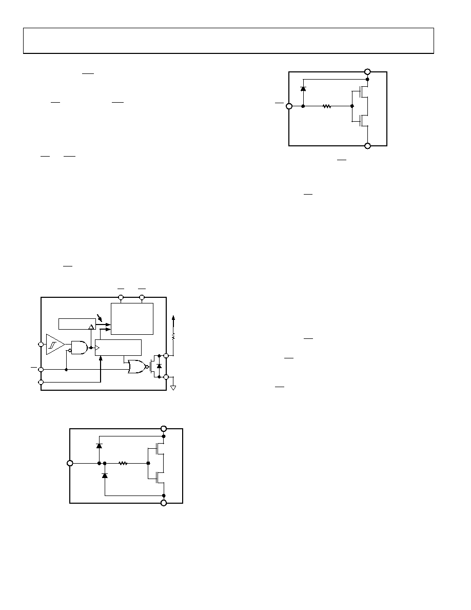
The equivalent serial data input and output logic is shown in
Figure 25. The open-drain output SDO is disabled whenever
chip-select (
AA
CSEE
AA
) is in logic high. ESD protection of the digital
inputs is shown in Figure 26 and Figure 27.
VALID
COMMAND
COUNTER
COMMAND
PROCESSOR
AND ADDRESS
DECODE
(FOR DAISY
CHAIN ONLY)
SERIAL
REGISTER
CLK
SDI
5V
RPULL-UP
SDO
GND
PR
WP
ADN2850
CS
0
2
6
0
-0
3
7
Figure 25. Equivalent Digital Input and Output Logic
LOGIC
PINS
VDD
GND
INPUTS
300
0
2
6
0
-0
3
8
Figure 26. Equivalent ESD Digital Input Protection
VDD
GND
INPUT
300
WP
0
2
6
0
-0
3
9
Figure 27. Equivalent
AA
WPEE
AA
Input Protection
SERIAL DATA INTERFACE
The ADN2850 contains a 4-wire SPI-compatible digital
interface (SDI, SDO,
AA
CSEE
AA
, and CLK). The 24-bit serial data-word
must be loaded with MSB first. The format of the word is shown in
Table 7. The command bits (C0 to C3) control the operation of the
digital resistor according to the command shown in Table 8. A0
to A3 are the address bits. A0 is used to address RDAC1 or RDAC2.
Address 2 to Address 14 are accessible by users for extra EEMEM.
Address 15 is reserved for factory usage. Table 10 provides an
address map of the EEMEM locations. D0 to D9 are the values
for the RDAC registers. D0 to D15 are the values for the EEMEM
registers.
The ADN2850 has an internal counter that counts a multiple of
24 bits (a frame) for proper operation. For example, ADN2850
works with a 24-bit or 48-bit word, but it cannot work properly
with a 23-bit or 25-bit word. To prevent data from mislocking
(due to noise, for example), the counter resets, if the count is not a
multiple of four when
AA
CSEE
AA
goes high but remains in the register if it
is multiple of four. In addition, the ADN2850 has a subtle
feature that, if
AA
CSEE
AA
is pulsed without CLK and SDI, the part
repeats the previous command (except during power-up). As a
result, care must be taken to ensure that no excessive noise exists in
the CLK or
AA
CSEE
AA
line that might alter the effective number-of-bits
pattern.
The SPI interface can be used in two slave modes: CPHA = 1,
CPOL = 1 and CPHA = 0, CPOL = 0. CPHA and CPOL refer to
the control bits that dictate SPI timing in the following
MicroConverters and microprocessors: ADuC812, ADuC824,
M68HC11, MC68HC16R1, and MC68HC916R1.
DAISY-CHAIN OPERATION
The serial data output pin (SDO) serves two purposes. It can be
used to read the contents of the wiper setting and EEMEM values
using Instruction 10 and Instruction 9, respectively. The remaining
instructions (Instruction 0 to Instruction 8, Instruction 11 to
Instruction 15) are valid for daisy-chaining multiple devices in
simultaneous operations. Daisy-chaining minimizes the number
of port pins required from the controlling IC (see Figure 28). The
SDO pin contains an open-drain N-Ch FET that requires a pull-up
resistor, if this function is used. As shown in Figure 28, users need
to tie the SDO pin of one package to the SDI pin of the next package.
Users may need to increase the clock period because the pull-up
相关PDF资料 |
PDF描述 |
|---|---|
| VE-B3J-MY-F4 | CONVERTER MOD DC/DC 36V 50W |
| AD5232BRU10 | IC DGTL POT 256POS 10K 16TSSOP |
| VI-2NW-MX-B1 | CONVERTER MOD DC/DC 5.5V 75W |
| VE-B3J-MY-F3 | CONVERTER MOD DC/DC 36V 50W |
| AD8403ARZ50 | IC DCP QUAD 50K 24-SOIC |
相关代理商/技术参数 |
参数描述 |
|---|---|
| ADN2850BCPZ250-RL7 | 功能描述:IC DGTL RHEO DL 25K 9BIT16LFCSP RoHS:是 类别:集成电路 (IC) >> 数据采集 - 数字电位器 系列:- 标准包装:3,000 系列:DPP 接片:32 电阻(欧姆):10k 电路数:1 温度系数:标准值 300 ppm/°C 存储器类型:非易失 接口:3 线串行(芯片选择,递增,增/减) 电源电压:2.5 V ~ 6 V 工作温度:-40°C ~ 85°C 安装类型:表面贴装 封装/外壳:8-WFDFN 裸露焊盘 供应商设备封装:8-TDFN(2x3) 包装:带卷 (TR) |
| ADN2850BCPZ25-RL7 | 功能描述:IC DGTL RHEO DL 25K 9BIT16LFCSP RoHS:是 类别:集成电路 (IC) >> 数据采集 - 数字电位器 系列:- 标准包装:3,000 系列:DPP 接片:32 电阻(欧姆):10k 电路数:1 温度系数:标准值 300 ppm/°C 存储器类型:非易失 接口:3 线串行(芯片选择,递增,增/减) 电源电压:2.5 V ~ 6 V 工作温度:-40°C ~ 85°C 安装类型:表面贴装 封装/外壳:8-WFDFN 裸露焊盘 供应商设备封装:8-TDFN(2x3) 包装:带卷 (TR) |
| ADN2850BRU25 | 制造商:Analog Devices 功能描述: |
| adn2850bru25-rl7 | 制造商:Analog Devices 功能描述: |
| ADN2850BRUZ25 | 制造商:Analog Devices 功能描述:DUAL 9-BIT SPI DIG. POT - Rail/Tube 制造商:Analog Devices 功能描述:Dual 10-B Progable Non-Volatile Resistor |
发布紧急采购,3分钟左右您将得到回复。