- 您现在的位置:买卖IC网 > PDF目录1776 > ADP1821ARQZ-R7 (Analog Devices Inc)IC REG CTRLR BUCK PWM VM 16-QSOP PDF资料下载
参数资料
| 型号: | ADP1821ARQZ-R7 |
| 厂商: | Analog Devices Inc |
| 文件页数: | 6/24页 |
| 文件大小: | 0K |
| 描述: | IC REG CTRLR BUCK PWM VM 16-QSOP |
| 标准包装: | 1 |
| PWM 型: | 电压模式 |
| 输出数: | 1 |
| 频率 - 最大: | 720kHz |
| 占空比: | 90% |
| 电源电压: | 3.7 V ~ 5.5 V |
| 降压: | 是 |
| 升压: | 无 |
| 回扫: | 无 |
| 反相: | 无 |
| 倍增器: | 无 |
| 除法器: | 无 |
| Cuk: | 无 |
| 隔离: | 无 |
| 工作温度: | -40°C ~ 85°C |
| 封装/外壳: | 16-SSOP(0.154",3.90mm 宽) |
| 包装: | 标准包装 |
| 产品目录页面: | 791 (CN2011-ZH PDF) |
| 其它名称: | ADP1821ARQZ-R7DKR |
�� ��
��
��ADP1821�
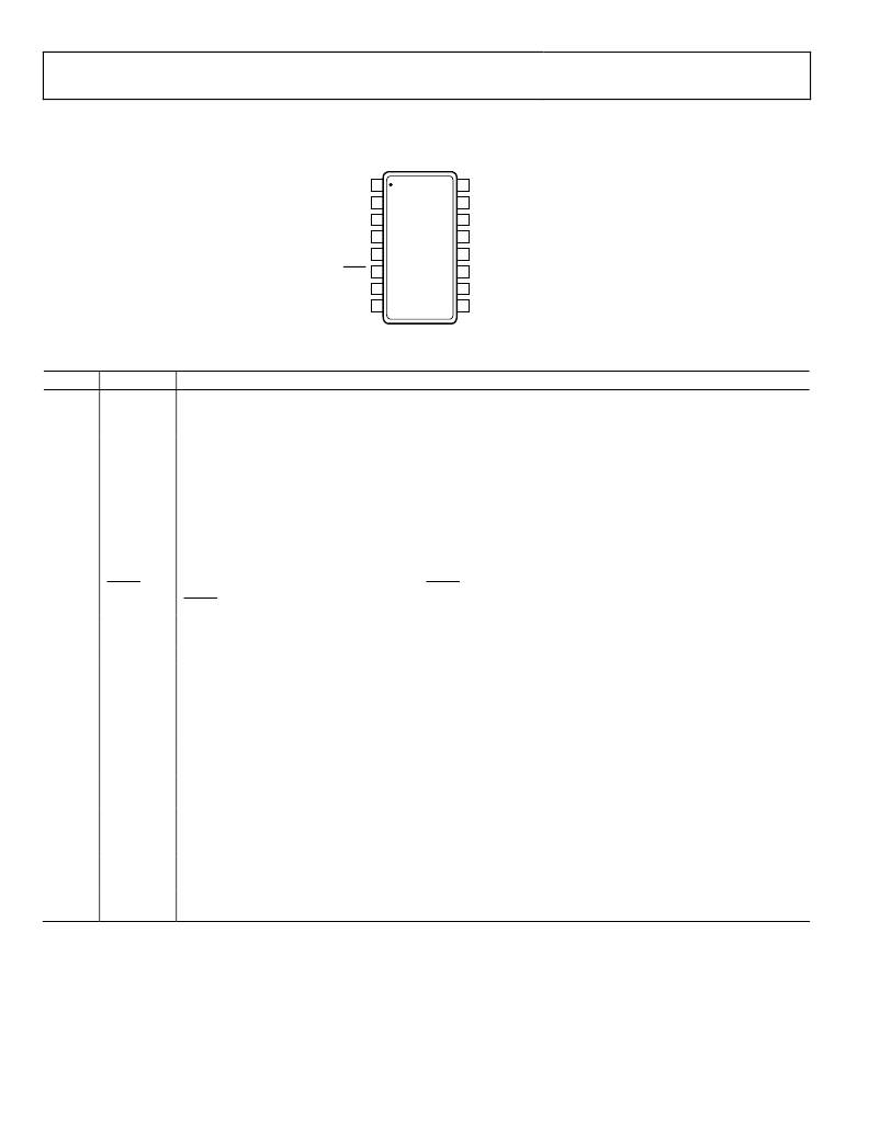
�PIN� CONFIGURATION� AND� FUNCTION� DESCRIPTIONS�
�BST�
�DH�
�1�
�2�
�16�
�15�
�PVCC�
�DL�
�SW�
�SYNC�
�FREQ�
�SHDN�
�3�
�4�
�5�
�6�
�ADP1821�
�TOP� VIEW�
�(Not� to� Scale)�
�14�
�13�
�12�
�11�
�PGND�
�CSL�
�VCC�
�COMP�
�PWGD� 7�
�10�
�FB�
�GND�
�8�
�9�
�SS�
�Figure� 4.� Pin� Configuration�
�Table� 3.� Pin� Function� Descriptions�
�Pin� No.�
�1�
�2�
�3�
�4�
�5�
�6�
�7�
�8�
�9�
�10�
�11�
�12�
�13�
�14�
�15�
�16�
�Mnemonic�
�BST�
�DH�
�SW�
�SYNC�
�FREQ�
�SHDN�
�PWGD�
�GND�
�SS�
�FB�
�COMP�
�VCC�
�CSL�
�PGND�
�DL�
�PVCC�
�Description�
�High-Side� Gate� Driver� Boost� Capacitor� Input.� A� capacitor� between� SW� and� BST� powers� the� high-side� gate� driver,� DH.�
�The� capacitor� is� charged� through� a� diode� from� PVCC� when� the� low-side� MOSFET� is� on.� Connect� a� 0.1� μF� or� greater�
�ceramic� capacitor� from� BST� to� SW� and� a� Schottky� diode� from� PVCC� to� BST� to� power� the� high-side� gate� driver.�
�High-Side� Gate� Driver� Output.� Connect� DH� to� the� gate� of� the� external� high-side,� N-channel� MOSFET� switch.� DH� is�
�powered� from� the� capacitor� between� SW� and� BST,� and� its� voltage� swings� between� V� SW� and� V� BST� .�
�Power� Switch� Node.� Connect� the� source� of� the� high-side,� N-channel� MOSFET� switch� and� the� drain� of� the� low-side,�
�N-channel� MOSFET� synchronous� rectifier� to� SW.� SW� powers� the� output� through� the� output� LC� filter.�
�Frequency� Synchronization� Input.� Drive� SYNC� with� an� external� 300� kHz� to� 1.2� MHz� signal� to� synchronize� the� converter�
�switching� frequency� to� the� applied� signal.� The� maximum� SYNC� frequency� is� limited� to� 2� times� the� nominal� internal�
�frequency� selected� by� FREQ.� Do� not� leave� SYNC� unconnected;� when� not� used,� connect� SYNC� to� GND.�
�Frequency� Select� Input.� FREQ� selects� the� converter� switching� frequency.� Drive� FREQ� low� to� select� 300� kHz,� or� high�
�to� select� 600� kHz.� Do� not� leave� FREQ� unconnected.�
�Active� Low,� DC-to-DC� Shutdown� Input.� Drive� SHDN� high� to� turn� on� the� converter� and� low� to� turn� it� off.� Connect�
�SHDN� to� VCC� for� automatic� startup.�
�Open-Drain,� Power-Good� Output.� PWGD� sinks� current� to� GND� when� the� output� voltage� is� above� or� below� the�
�regulation� voltage.� Connect� a� pull-up� resistor� from� PWGD� to� VDD� for� a� logical� power-good� indicator.�
�Analog� Ground.� Connect� GND� to� PGND� at� a� single� point� as� close� as� possible� to� the� internal� circuitry� (IC).�
�Soft� Start� Control� Input.� A� capacitor� from� SS� to� GND� controls� the� soft� start� period.� When� the� output� is� overloaded,�
�SS� is� discharged� to� prevent� excessive� input� current� while� the� output� recovers.� Connect� a� 1� nF� capacitor� to� a� 1� μF�
�capacitor� from� SS� to� GND� to� set� the� soft� start� period.� See� the� Soft� Start� section.�
�Voltage� Feedback� Input.� Connect� to� a� resistive� voltage� divider� from� the� output� to� FB� to� set� the� output� voltage.� See�
�the� Setting� the� Output� Voltage� section.�
�Compensation� Node.� Connect� a� resistor-capacitor� network� from� COMP� to� FB� to� compensate� the� regulation� control�
�system.� See� the� Compensation� section.�
�Internal� Power� Supply� Input.� VCC� powers� the� internal� circuitry.� Bypass� VCC� to� GND� with� a� 0.1� μF� or� greater�
�capacitor� connected� as� close� as� possible� to� the� IC.�
�Low-Side� Current� Sense� Input.� Connect� CSL� to� SW� through� a� resistor� to� set� the� current� limit.� See� the� Setting� the�
��Power� Ground.� Connect� GND� to� PGND� at� a� single� point� as� close� as� possible� to� the� IC.�
�Low-Side� Gate� Driver� Output.� Connect� DL� to� the� gate� of� the� low-side,� N-channel� MOSFET� synchronous� rectifier.� The�
�DL� voltage� swings� between� PGND� and� PVCC.�
�Internal� Gate� Driver� Power� Supply� Input.� PVCC� powers� the� low-side� gate� driver,� DL.� Bypass� PVCC� to� PGND� with� a�
�1� μF� or� greater� capacitor� connected� as� close� as� possible� to� the� IC.�
�Rev.� C� |� Page� 6� of� 24�
�相关PDF资料 |
PDF描述 |
|---|---|
| ADP1822ARQZ-R7 | IC REG CTRLR BUCK PWM VM 24-QSOP |
| ADP1823ACPZ-R7 | IC REG CTRLR BUCK PWM VM 32LFCSP |
| ADP1828ACPZ-R7 | IC REG CTRLR BUCK PWM VM 20LFCSP |
| ADP1829ACPZ-R7 | IC REG CTRLR BUCK PWM VM 32LFCSP |
| ADP1850ACPZ-R7 | IC REG CTRLR BUCK PWM CM 32LFCSP |
相关代理商/技术参数 |
参数描述 |
|---|---|
| ADP1821-BL1-EVZ | 制造商:Analog Devices 功能描述:Evaluation Board For Step-Down DC-To-DC Controller 制造商:Analog Devices 功能描述:BLANK ADISIMPOWER EVAL ADP1821 - Boxed Product (Development Kits) |
| ADP1821-BL2-EVZ | 制造商:Analog Devices 功能描述:Evaluation Board For Step-Down DC-To-DC Controller 制造商:Analog Devices 功能描述:BLANK ADISIMPOWER EVAL ADP1821 - Boxed Product (Development Kits) |
| ADP1821-EVAL | 功能描述:电源管理IC开发工具 Evaluation Board I.C. RoHS:否 制造商:Maxim Integrated 产品:Evaluation Kits 类型:Battery Management 工具用于评估:MAX17710GB 输入电压: 输出电压:1.8 V |
| ADP1822 | 制造商:AD 制造商全称:Analog Devices 功能描述:PWM, Step-Down DC-to-DC Controller with Margining and Tracking |
| ADP1822ARQZ-R7 | 功能描述:IC REG CTRLR BUCK PWM VM 24-QSOP RoHS:是 类别:集成电路 (IC) >> PMIC - 稳压器 - DC DC 切换控制器 系列:- 标准包装:75 系列:- PWM 型:电流模式 输出数:1 频率 - 最大:1MHz 占空比:81% 电源电压:4.3 V ~ 13.5 V 降压:是 升压:是 回扫:是 反相:无 倍增器:无 除法器:无 Cuk:无 隔离:无 工作温度:0°C ~ 70°C 封装/外壳:8-SOIC(0.154",3.90mm 宽) 包装:管件 产品目录页面:1051 (CN2011-ZH PDF) 其它名称:296-2543-5 |
发布紧急采购,3分钟左右您将得到回复。