- 您现在的位置:买卖IC网 > PDF目录15363 > ADP1883ARMZ-1.0-R7 (Analog Devices Inc)IC REG CTRLR BUCK PWM CM 10-MSOP PDF资料下载
参数资料
| 型号: | ADP1883ARMZ-1.0-R7 |
| 厂商: | Analog Devices Inc |
| 文件页数: | 22/40页 |
| 文件大小: | 0K |
| 描述: | IC REG CTRLR BUCK PWM CM 10-MSOP |
| 标准包装: | 1 |
| PWM 型: | 电流模式 |
| 输出数: | 1 |
| 频率 - 最大: | 1MHz |
| 占空比: | 45% |
| 电源电压: | 2.75 V ~ 20 V |
| 降压: | 是 |
| 升压: | 无 |
| 回扫: | 无 |
| 反相: | 无 |
| 倍增器: | 无 |
| 除法器: | 无 |
| Cuk: | 无 |
| 隔离: | 无 |
| 工作温度: | -40°C ~ 125°C |
| 封装/外壳: | 10-TFSOP,10-MSOP(0.118",3.00mm 宽) |
| 包装: | 标准包装 |
| 其它名称: | ADP1883ARMZ-1.0-R7DKR |
第1页第2页第3页第4页第5页第6页第7页第8页第9页第10页第11页第12页第13页第14页第15页第16页第17页第18页第19页第20页第21页当前第22页第23页第24页第25页第26页第27页第28页第29页第30页第31页第32页第33页第34页第35页第36页第37页第38页第39页第40页
�� �
�
�ADP1882/ADP1883�
�SYNCHRONOUS� RECTIFIER�
�The� ADP1882/ADP1883� employ� an� internal� lower-side� MOSFET�
�driver� to� drive� the� external� upper-side� and� lower-side� MOSFETs.�
�The� synchronous� rectifier� not� only� improves� overall� conduction�
�efficiency� but� also� ensures� proper� charging� to� the� bootstrap�
�capacitor� located� at� the� upper-side� driver� input.� This� is� beneficial�
�during� startup� to� provide� a� sufficient� drive� signal� to� the� external�
�upper-side� MOSFET� and� attain� a� fast� turn� on� response,� which� is�
�essential� for� minimizing� switching� losses.� The� integrated� upper-�
�side� and� lower-side� MOSFET� drivers� operate� in� complementary�
�fashion� with� built-in� anticross� conduction� circuitry� to� prevent�
�unwanted� shoot-through� current� that� may� potentially� damage� the�
�As� soon� as� the� forward� current� through� the� lower-side�
�MOSFET� decreases� to� a� level� where�
�10� mV� =� I� Q2� � R� ON(Q2)�
�the� zero-cross� comparator� (or� I� REV� comparator)� emits� a� signal� to�
�turn� off� the� lower-side� MOSFET.� From� this� point,� the� slope� of� the�
��as� the� body� diode� of� the� lower-side� MOSFET� begins� to� conduct�
�current� and� continues� conducting� current� until� the� remaining�
�energy� stored� in� the� inductor� has� been� depleted.�
�ANOTHER� t� ON� EDGE� IS�
�TRIGGERED� WHEN� V� OUT�
�FALLS� BELOW� REGULATION�
�MOSFETs� or� reduce� efficiency� as� a� result� of� excessive� power� loss.�
�POWER� SAVING� MODE� (PSM)� VERSION� (ADP1883)�
�The� ADP1883� is� the� power� saving� mode� version� of� the� ADP1882.�
�The� ADP1883� operates� in� the� discontinuous� conduction� mode�
�(DCM)� and� pulse� skips� at� light� load� to� midload� currents.� It� outputs�
�pulses,� as� necessary,� to� maintain� output� regulation.� Unlike� the�
�continuous� conduction� mode� (CCM),� DCM� operation� prevents�
�negative� current,� thus� allowing� improved� system� efficiency� at�
�light� loads.� Current� in� the� reverse� direction� through� this� pathway,�
�however,� results� in� power� dissipation� and,� therefore,� a� decrease�
�in� efficiency.�
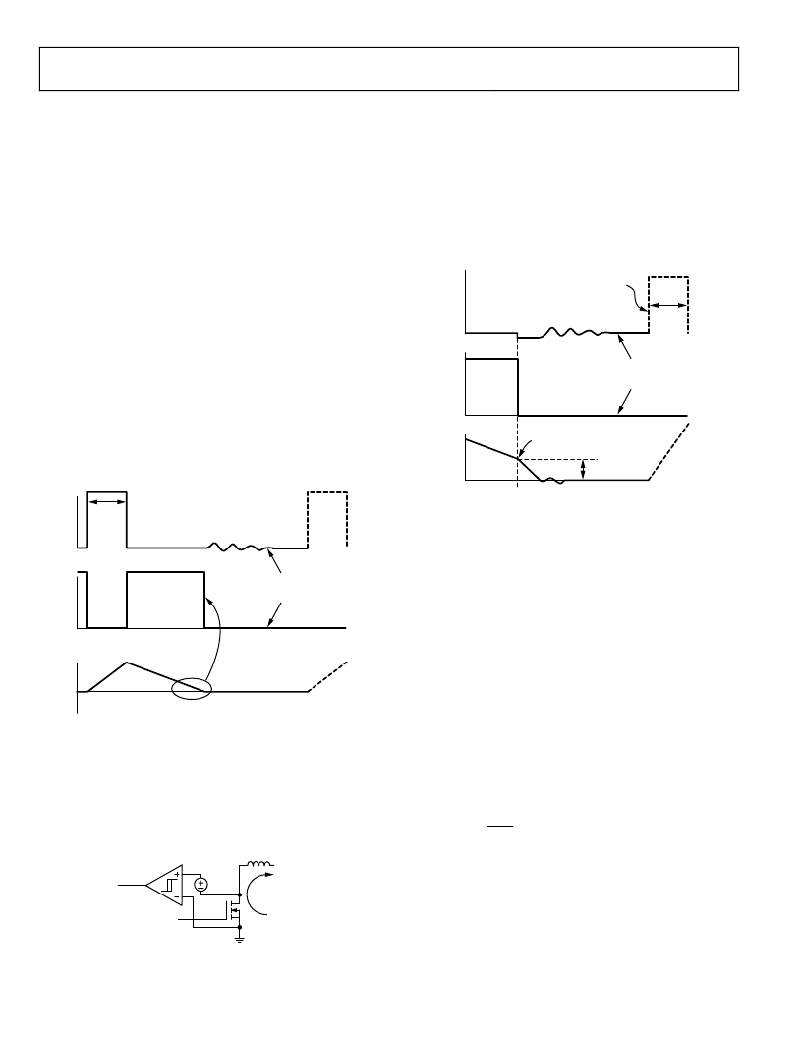
�SW�
�LS�
�I� LOAD�
�0A�
�t� ON�
�HS� AND� LS�
�IN� IDLE� MODE�
�ZERO-CROSS� COMPARATOR�
�DETECTS� 10mV� OFFSET� AND�
�TURNS� OFF� LS�
�10mV� =� R� ON� � I� LOAD�
�HS�
�t� ON�
�Figure� 76.� 10� mV� Offset� to� Ensure� Prevention� of� Negative� Inductor� Current�
�The� system� remains� in� idle� mode� until� the� output� voltage� drops�
�from� within� regulation.� A� PWM� pulse� is� then� produced,� turning�
�on� the� upper-side� MOSFET� to� maintain� system� regulation.� The�
�LS�
�t� OFF�
�HS� AND� LS� ARE� OFF�
�OR� IN� IDLE� MODE�
�ADP1883� does� not� have� an� internal� clock;� therefore,� it� switches�
�purely� as� a� hysteretic� controller� as� described� in� this� section.�
�TIMER� OPERATION�
�The� ADP1882/ADP1883� employ� a� constant� on-time� architecture�
�I� LOAD�
�0A�
�AS� THE� INDUCTOR�
�CURRENT� APPROACHES�
�ZERO� CURRENT,� THE� STATE�
�MACHINE� TURNS� OFF� THE�
�LOWER-SIDE� MOSFET.�
�that� provides� a� variety� of� benefits,� including� improved� load� and�
�line� transient� responses� when� compared� with� a� constant� (fixed)�
�frequency� current-mode� control� loop� of� a� comparable� loop� design.�
�The� constant� on-time� timer,� or� t� ON� timer,� senses� the� high� input�
�Figure� 74.� Discontinuous� Mode� of� Operation� (DCM)�
�To� minimize� the� chance� of� negative� inductor� current� buildup,�
�an� on-board,� zero-cross� comparator� turns� off� all� upper-side� and�
�lower-side� switching� activities� when� the� inductor� current�
�approaches� the� zero� current� line,� causing� the� system� to� enter�
�voltage� (V� IN� )� and� the� output� voltage� (V� OUT� )� using� SW� waveform�
�information� to� produce� an� adjustable� one-shot� PWM� pulse� that�
�varies� the� on� time� of� the� upper-side� MOSFET� in� response� to�
�dynamic� changes� in� input� voltage,� output� voltage,� and� load� current�
�conditions� to� maintain� regulation.� It� then� generates� an� on-time�
�(t� ON� )� pulse� that� is� inversely� proportional� to� V� IN� .�
�idle� mode,� where� the� upper-side� and� lower-side� MOSFETs� are�
�turned� off.� To� ensure� idle� mode� entry,� a� 10� mV� offset,� connected�
�in� series� at� the� SW� node,� is� implemented� (see� Figure� 75).�
�t� ON� =� K� �
�V� OUT�
�V� IN�
�ZERO-CROSS�
�COMPARATOR�
�SW�
�I� Q2�
�where� K� is� a� constant� that� is� trimmed� using� an� RC� timer� product�
�for� the� 300� kHz,� 600� kHz,� and� 1.0� MHz� frequency� options.�
�10mV�
�LS�
�Q2�
�Figure� 75.� Zero-Cross� Comparator� with� 10� mV� of� Offset�
�Rev.� 0� |� Page� 22� of� 40�
�相关PDF资料 |
PDF描述 |
|---|---|
| RCM30DCAD-S189 | CONN EDGECARD 60POS R/A .156 SLD |
| VE-J14-EW-F3 | CONVERTER MOD DC/DC 48V 100W |
| H2BXG-10105-V8-ND | JUMPER-H1501TR/A3048V/X 5" |
| VE-J14-EW-F1 | CONVERTER MOD DC/DC 48V 100W |
| GSM15DTBS-S189 | CONN EDGECARD 30POS R/A .156 SLD |
相关代理商/技术参数 |
参数描述 |
|---|---|
| ADP190 | 制造商:AD 制造商全称:Analog Devices 功能描述:Logic Controlled, High-Side Power Switches |
| ADP190ACBZ-R7 | 功能描述:IC CTRLR HIGH SIDE PWR SW 4WLCSP RoHS:是 类别:集成电路 (IC) >> PMIC - MOSFET,电桥驱动器 - 内部开关 系列:- 标准包装:2,500 系列:- 类型:高端 输入类型:非反相 输出数:1 导通状态电阻:35 毫欧 电流 - 输出 / 通道:- 电流 - 峰值输出:3A 电源电压:2.7 V ~ 5.5 V 工作温度:-40°C ~ 85°C 安装类型:表面贴装 封装/外壳:14-TSSOP(0.173",4.40mm 宽) 供应商设备封装:14-TSSOP 包装:带卷 (TR) 其它名称:MIC2545A-1YTSTRMIC2545A-1YTSTR-ND |
| ADP190CB-EVALZ | 功能描述:BOARD EVAL ADP190 RoHS:是 类别:编程器,开发系统 >> 评估演示板和套件 系列:- 标准包装:1 系列:- 主要目的:数字电位器 嵌入式:- 已用 IC / 零件:AD5258 主要属性:- 次要属性:- 已供物品:板 相关产品:AD5258BRMZ1-ND - IC POT DGTL I2C1K 64P 10MSOPAD5258BRMZ10-ND - IC POT DGTL I2C 10K 64P 10MSOPAD5258BRMZ100-ND - IC POT DGTL I2C 100K 64P 10MSOPAD5258BRMZ50-ND - IC POT DGTL I2C 50K 64P 10MSOPAD5258BRMZ1-R7-ND - IC POT DGTL I2C 1K 64P 10MSOPAD5258BRMZ10-R7-ND - IC POT DGTL I2C 10K 64P 10MSOPAD5258BRMZ50-R7-ND - IC POT DGTL I2C 50K 64P 10MSOPAD5258BRMZ100-R7-ND - IC POT DGTL I2C 100K 64P 10MSOP |
| ADP191ACBZ-R7 | 功能描述:IC CTLR HIGH LSIDE PWR SW 4WLCSP RoHS:是 类别:集成电路 (IC) >> PMIC - MOSFET,电桥驱动器 - 内部开关 系列:- 标准包装:2,500 系列:- 类型:高端 输入类型:非反相 输出数:1 导通状态电阻:35 毫欧 电流 - 输出 / 通道:- 电流 - 峰值输出:3A 电源电压:2.7 V ~ 5.5 V 工作温度:-40°C ~ 85°C 安装类型:表面贴装 封装/外壳:14-TSSOP(0.173",4.40mm 宽) 供应商设备封装:14-TSSOP 包装:带卷 (TR) 其它名称:MIC2545A-1YTSTRMIC2545A-1YTSTR-ND |
| ADP191CB-EVALZ | 功能描述:EVAL BOARD FOR ADP191 RoHS:是 类别:编程器,开发系统 >> 评估演示板和套件 系列:- 标准包装:1 系列:- 主要目的:电信,线路接口单元(LIU) 嵌入式:- 已用 IC / 零件:IDT82V2081 主要属性:T1/J1/E1 LIU 次要属性:- 已供物品:板,电源,线缆,CD 其它名称:82EBV2081 |
发布紧急采购,3分钟左右您将得到回复。