- 您现在的位置:买卖IC网 > PDF目录298814 > ADS1298RIZXGT (TEXAS INSTRUMENTS INC) SPECIALTY ANALOG CIRCUIT, PBGA64 PDF资料下载
参数资料
| 型号: | ADS1298RIZXGT |
| 厂商: | TEXAS INSTRUMENTS INC |
| 元件分类: | 模拟信号调理 |
| 英文描述: | SPECIALTY ANALOG CIRCUIT, PBGA64 |
| 封装: | 8 X 8 MM, LEAD FREE, PLASTIC, NFBGA-64 |
| 文件页数: | 38/87页 |
| 文件大小: | 1430K |
| 代理商: | ADS1298RIZXGT |
第1页第2页第3页第4页第5页第6页第7页第8页第9页第10页第11页第12页第13页第14页第15页第16页第17页第18页第19页第20页第21页第22页第23页第24页第25页第26页第27页第28页第29页第30页第31页第32页第33页第34页第35页第36页第37页当前第38页第39页第40页第41页第42页第43页第44页第45页第46页第47页第48页第49页第50页第51页第52页第53页第54页第55页第56页第57页第58页第59页第60页第61页第62页第63页第64页第65页第66页第67页第68页第69页第70页第71页第72页第73页第74页第75页第76页第77页第78页第79页第80页第81页第82页第83页第84页第85页第86页第87页
1
9
17
25
CS
SCLK
DIN
OPCODE1
OPCODE2
DOUT
REGDATA
REGDATA+1
1
9
17
25
CS
SCLK
DIN
OPCODE1
OPCODE2
REGDATA1
REGDATA2
DOUT
SBAS459H
– JANUARY 2010 – REVISED MAY 2011
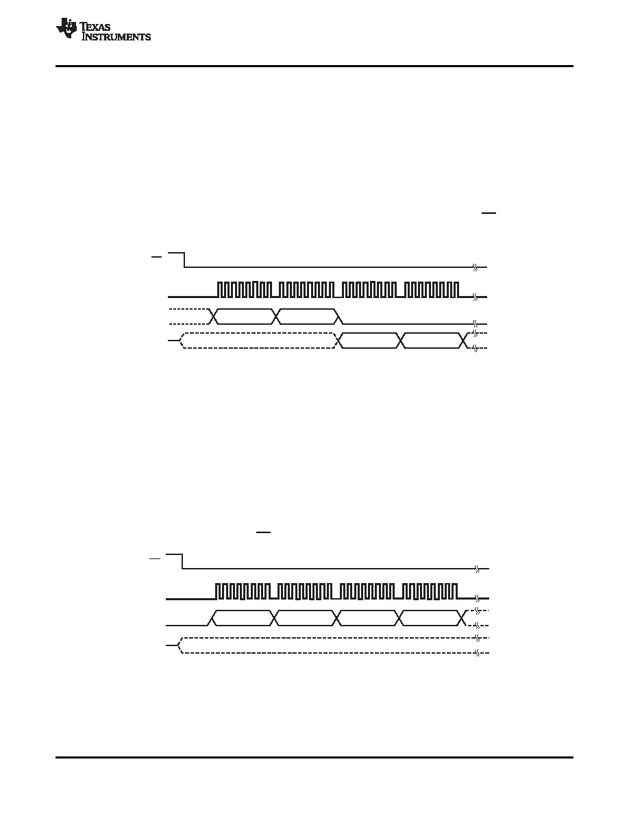
RREG: Read From Register
This opcode reads register data. The Register Read command is a two-byte opcode followed by the output of the
register data. The first byte contains the command opcode and the register address. The second byte of the
opcode specifies the number of registers to read
– 1.
First opcode byte: 001r rrrr, where r rrrr is the starting register address.
Second opcode byte: 000n nnnn, where n nnnn is the number of registers to read
– 1.
The 17th SCLK rising edge of the operation clocks out the MSB of the first register, as shown in Figure 49. When
the device is in read data continuous mode, it is necessary to issue a SDATAC command before a RREG
command can be issued. An RREG command can be issued any time. However, because this command is a
multi-byte command, there are restrictions on the SCLK rate depending on the way the SCLKs are issued. See
the Serial Clock (SCLK) subsection of the SPI Interface section for more details. Note that CS must be low for
the entire command.
Figure 49. RREG Command Example: Read Two Registers Starting from Register 00h (ID Register)
(OPCODE 1 = 0010 0000, OPCODE 2 = 0000 0001)
WREG: Write to Register
This opcode writes register data. The Register Write command is a two-byte opcode followed by the input of the
register data. The first byte contains the command opcode and the register address.
The second byte of the opcode specifies the number of registers to write
– 1.
First opcode byte: 010r rrrr, where r rrrr is the starting register address.
Second opcode byte: 000n nnnn, where n nnnn is the number of registers to write
– 1.
After the opcode bytes, the register data follows (in MSB-first format), as shown in Figure 50. WREG command
can be issued any time. However, because this command is a multi-byte command, there are restrictions on the
SCLK rate depending on the way the SCLKs are issued. See the Serial Clock (SCLK) subsection of the SPI
Interface section for more details. Note that CS must be low for the entire command.
Figure 50. WREG Command Example: Write Two Registers Starting from 00h (ID Register)
(OPCODE 1 = 0100 0000, OPCODE 2 = 0000 0001)
Copyright
2010–2011, Texas Instruments Incorporated
43
相关PDF资料 |
PDF描述 |
|---|---|
| ADSP-1401TN/883B | 16-BIT, MICROPROGRAM SEQUENCER, PDIP48 |
| ADSP-21160NCB-100 | 64-BIT, 50 MHz, OTHER DSP, PBGA400 |
| ADSP-21365YSWZ-2BA | 16-BIT, 55.55 MHz, OTHER DSP, PQFP144 |
| ADSP-2181BS-160 | 24-BIT, 20 MHz, OTHER DSP, PQFP128 |
| ADUC845BCPZ8-3 | 8-BIT, FLASH, 12.58 MHz, MICROCONTROLLER, QCC56 |
相关代理商/技术参数 |
参数描述 |
|---|---|
| ADS1299 | 制造商:TI 制造商全称:Texas Instruments 功能描述:Low-Noise, 8-Channel, 24-Bit Analog Front-End for Biopotential Measurements |
| ADS1299_1211 | 制造商:TI 制造商全称:Texas Instruments 功能描述:Low-Noise, 8-Channel, 24-Bit Analog Front-End for Biopotential Measurements |
| ADS1299-4PAG | 功能描述:IC AFE 4-CH 24BIT 64TQFP 制造商:texas instruments 系列:- 包装:托盘 零件状态:在售 位数:24 通道数:4 电压 - 电源,模拟:5V 电压 - 电源,数字:1.8 V ~ 3.6 V 封装/外壳:64-TQFP 供应商器件封装:64-TQFP(10x10) 标准包装:160 |
| ADS1299-4PAGR | 功能描述:IC AFE 4-CH 24BIT 64TQFP 制造商:texas instruments 系列:- 包装:剪切带(CT) 零件状态:在售 位数:24 通道数:4 功率(W):24mW 电压 - 电源,模拟:4.75 V ~ 5.25 V 电压 - 电源,数字:1.8 V ~ 3.6 V 封装/外壳:64-TQFP 供应商器件封装:64-TQFP(10x10) 标准包装:1 |
| ADS1299-6PAG | 功能描述:IC AFE 6-CH 24BIT 64TQFP 制造商:texas instruments 系列:- 包装:托盘 零件状态:在售 位数:24 通道数:6 功率(W):33mW 电压 - 电源,模拟:5V 电压 - 电源,数字:1.8 V ~ 3.6 V 封装/外壳:64-TQFP 供应商器件封装:64-TQFP(10x10) 标准包装:160 |
发布紧急采购,3分钟左右您将得到回复。