- 您现在的位置:买卖IC网 > PDF目录19466 > ADSP-21065LKSZ-240 (Analog Devices Inc)IC DSP CONTROLLR 544KBIT 208MQFP PDF资料下载
参数资料
| 型号: | ADSP-21065LKSZ-240 |
| 厂商: | Analog Devices Inc |
| 文件页数: | 23/44页 |
| 文件大小: | 0K |
| 描述: | IC DSP CONTROLLR 544KBIT 208MQFP |
| 产品培训模块: | SHARC Processor Overview |
| 标准包装: | 1 |
| 系列: | SHARC® |
| 类型: | 浮点 |
| 接口: | 主机接口,串行端口 |
| 时钟速率: | 60MHz |
| 非易失内存: | 外部 |
| 芯片上RAM: | 64kB |
| 电压 - 输入/输出: | 3.30V |
| 电压 - 核心: | 3.30V |
| 工作温度: | 0°C ~ 85°C |
| 安装类型: | 表面贴装 |
| 封装/外壳: | 208-BFQFP |
| 供应商设备封装: | 208-MQFP(28x28) |
| 包装: | 托盘 |
| 其它名称: | ADSP-21065LKSZ240 ADSP-21065LKSZ240-ND |
第1页第2页第3页第4页第5页第6页第7页第8页第9页第10页第11页第12页第13页第14页第15页第16页第17页第18页第19页第20页第21页第22页当前第23页第24页第25页第26页第27页第28页第29页第30页第31页第32页第33页第34页第35页第36页第37页第38页第39页第40页第41页第42页第43页第44页
REV. C
ADSP-21065L
–3–
GENERAL DESCRIPTION
The ADSP-21065L is a powerful member of the SHARC
family of 32-bit processors optimized for cost sensitive appli-
cations. The SHARC—Super Harvard Architecture—offers the
highest levels of performance and memory integration of any
32-bit DSP in the industry—they are also the only DSP in the
industry that offer both fixed and floating-point capabilities,
without compromising precision or performance.
The ADSP-21065L is fabricated in a high speed, low power
CMOS process, 0.35
mm technology. With its on-chip instruc-
tion cache, the processor can execute every instruction in a
single cycle. Table I lists the performance benchmarks for the
ADSP-21065L.
The ADSP-21065L SHARC combines a floating-point DSP
core with integrated, on-chip system features, including a
544 Kbit SRAM memory, host processor interface, DMA con-
troller, SDRAM controller, and enhanced serial ports.
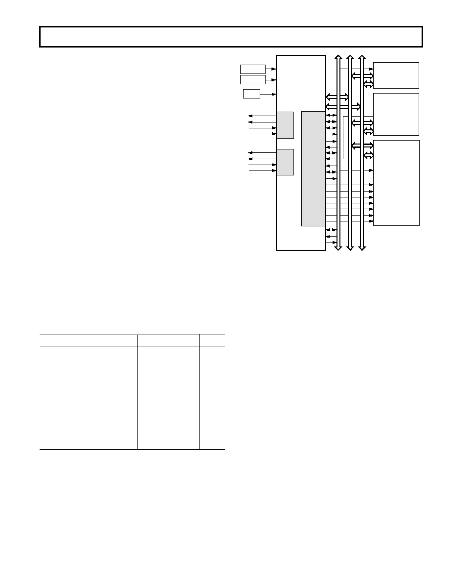
Figure 1 shows a block diagram of the ADSP-21065L, illustrat-
ing the following architectural features:
Computation Units (ALU, Multiplier, and Shifter) with a
Shared Data Register File
Data Address Generators (DAG1, DAG2)
Program Sequencer with Instruction Cache
Timers with Event Capture Modes
On-Chip, dual-ported SRAM
External Port for Interfacing to Off-Chip Memory and
Peripherals
Host Port and SDRAM Interface
DMA Controller
Enhanced Serial Ports
JTAG Test Access Port
Table I. Performance Benchmarks
Benchmark
Timing
Cycles
Cycle Time
15.00 ns
1
1024-Pt. Complex FFT
(Radix 4, with Digit Reverse)
0.274 ns
18221
Matrix Multiply (Pipelined)
[3
3] [3 1]
135 ns
9
[4
4] [4 1]
240 ns
16
FIR Filter (per Tap)
15 ns
1
IIR Filter (per Biquad)
60 ns
4
Divide Y/X
90 ns
6
Inverse Square Root (1/
÷x)
135 ns
9
DMA Transfers
264 Mbytes/sec.
ADSP-21000 FAMILY CORE ARCHITECTURE
The ADSP-21065L is code and function compatible with the
ADSP-21060/ADSP-21061/ADSP-21062. The ADSP-21065L
includes the following architectural features of the SHARC
family core.
RESET
ADSP-21065L
#1
BMS
ADDR23-0
DATA31-0
CONTROL
ADDRESS
DATA
CS
ADDR
DATA
BOOT
EPROM
(OPTIONAL)
ADDR
SDRAM
(OPTIONAL)
DATA
ADDR
DATA
HOST
PROCESSOR
(OPTIONAL)
CLOCK
CS
HBR
HBG
REDY
RD
WR
ACK
SBTS
SW
BR2
CLKIN
MS3-0
CPA
CS
RESET
ID1-0
01
TX0_A
TX0_B
RX0_A
RX0_B
SPORT0
TX1_A
TX1_B
RX1_A
RX1_B
SPORT1
CS
RAS
CAS
DQM
SDCLK1-0
SDCKE
SDA10
BR1
RAS
CAS
DQM
CLK
CKE
A10
CONTROL
SDWE
WE
Figure 2. ADSP-21065L Single-Processor System
Independent, Parallel Computation Units
The arithmetic/logic unit (ALU), multiplier, and shifter all
perform single-cycle instructions. The three units are arranged
in parallel, maximizing computational throughput. Single multi-
function instructions execute parallel ALU and multiplier
operations. These computation units support IEEE 32-bit
single-precision floating-point, extended precision 40-bit floating-
point, and 32-bit fixed-point data formats.
Data Register File
A general-purpose data register file is used for transferring data
between the computation units and the data buses, and for
storing intermediate results. This 10-port, 32-register (16 primary,
16 secondary) register file, combined with the ADSP-21000
Harvard architecture, allows unconstrained data flow between
computation units and internal memory.
Single-Cycle Fetch of Instruction and Two Operands
The ADSP-21065L features an enhanced Super Harvard Archi-
tecture in which the data memory (DM) bus transfers data and
the program memory (PM) bus transfers both instructions and
data (see Figure 1). With its separate program and data memory
buses, and on-chip instruction cache, the processor can simulta-
neously fetch two operands and an instruction (from the cache),
all in a single cycle.
Instruction Cache
The ADSP-21065L includes an on-chip instruction cache that
enables three-bus operation for fetching an instruction and two
data values. The cache is selective—only the instructions that
fetches conflict with PM bus data accesses are cached. This
allows full-speed execution of core, looped operations such as
digital filter multiply-accumulates and FFT butterfly processing.
Data Address Generators with Hardware Circular Buffers
The ADSP-21065L’s two data address generators (DAGs)
implement circular data buffers in hardware. Circular buffers
allow efficient programming of delay lines and other data
相关PDF资料 |
PDF描述 |
|---|---|
| GEC07DRTI | CONN EDGECARD 14POS DIP .100 SLD |
| TAP106M035DCS | CAP TANT 10UF 35V 20% RADIAL |
| HMM36DRTF | CONN EDGECARD 72POS DIP .156 SLD |
| VI-B12-CW-B1 | CONVERTER MOD DC/DC 15V 100W |
| VE-21K-CY-F3 | CONVERTER MOD DC/DC 40V 50W |
相关代理商/技术参数 |
参数描述 |
|---|---|
| ADSP-21065LKSZ-264 | 功能描述:IC DSP CONTROLL 544KBIT 208-MQFP RoHS:是 类别:集成电路 (IC) >> 嵌入式 - DSP(数字式信号处理器) 系列:SHARC® 标准包装:40 系列:TMS320DM64x, DaVinci™ 类型:定点 接口:I²C,McASP,McBSP 时钟速率:400MHz 非易失内存:外部 芯片上RAM:160kB 电压 - 输入/输出:3.30V 电压 - 核心:1.20V 工作温度:0°C ~ 90°C 安装类型:表面贴装 封装/外壳:548-BBGA,FCBGA 供应商设备封装:548-FCBGA(27x27) 包装:托盘 配用:TMDSDMK642-0E-ND - DEVELPER KIT W/NTSC CAMERA296-23038-ND - DSP STARTER KIT FOR TMS320C6416296-23059-ND - FLASHBURN PORTING KIT296-23058-ND - EVAL MODULE FOR DM642TMDSDMK642-ND - DEVELOPER KIT W/NTSC CAMERA |
| ADSP-2106X | 制造商:AD 制造商全称:Analog Devices 功能描述:DSP Microcomputer Family |
| ADSP-2109 | 制造商:AD 制造商全称:Analog Devices 功能描述:Low Cost DSP Microcomputers |
| ADSP-2109KP-80 | 制造商:AD 制造商全称:Analog Devices 功能描述:Low Cost DSP Microcomputers |
| ADSP-2109LKP-55 | 制造商:AD 制造商全称:Analog Devices 功能描述:Low Cost DSP Microcomputers |
发布紧急采购,3分钟左右您将得到回复。