参数资料
| 型号: | ADSP-3PARCBF548M01 |
| 厂商: | Analog Devices Inc |
| 文件页数: | 57/100页 |
| 文件大小: | 0K |
| 描述: | MODULE BOARD BF548 |
| 产品培训模块: | Arcturus uCBF54x-EMM |
| 特色产品: | uCBF54x Start Kit and System Module by Arcturus |
| 标准包装: | 5 |
| 系列: | Blackfin® |
| 模块/板类型: | 处理器模块 |
| 适用于相关产品: | ADSP-BF548 |
| 相关产品: | ADSP-BF548MBBCZ-5M-ND - IC DSP 533MHZ W/DDR 400CSPBGA ADSP-BF548BBCZ-5A-ND - IC DSP 16BIT 533MHZ 400CSBGA |
第1页第2页第3页第4页第5页第6页第7页第8页第9页第10页第11页第12页第13页第14页第15页第16页第17页第18页第19页第20页第21页第22页第23页第24页第25页第26页第27页第28页第29页第30页第31页第32页第33页第34页第35页第36页第37页第38页第39页第40页第41页第42页第43页第44页第45页第46页第47页第48页第49页第50页第51页第52页第53页第54页第55页第56页当前第57页第58页第59页第60页第61页第62页第63页第64页第65页第66页第67页第68页第69页第70页第71页第72页第73页第74页第75页第76页第77页第78页第79页第80页第81页第82页第83页第84页第85页第86页第87页第88页第89页第90页第91页第92页第93页第94页第95页第96页第97页第98页第99页第100页
Rev. C
|
Page 6 of 100
|
February 2010
ADSP-BF542/ADSP-BF544/ADSP-BF547/ADSP-BF548/ADSP-BF549
MEMORY ARCHITECTURE
The ADSP-BF54x processors view memory as a single unified
4G byte address space, using 32-bit addresses. All resources,
including internal memory, external memory, and I/O control
registers, occupy separate sections of this common address
space. The memory portions of this address space are arranged
in a hierarchical structure to provide a good cost/performance
balance of some very fast, low-latency on-chip memory as cache
or SRAM, and larger, lower-cost and performance off-chip
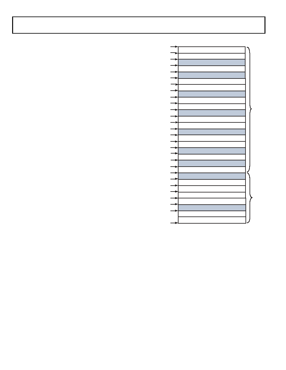
memory systems. See Figure 3 on Page 6.
The on-chip L1 memory system is the highest-performance
memory available to the Blackfin processor. The off-chip mem-
ory system, accessed through the external bus interface unit
(EBIU), provides expansion with flash memory, SRAM, and
double-rate SDRAM (standard or mobile DDR), optionally
accessing up to 768M bytes of physical memory.
Most of the ADSP-BF54x Blackfin processors also include an L2
SRAM memory array which provides up to 128K bytes of high
speed SRAM, operating at one half the frequency of the core and
with slightly longer latency than the L1 memory banks (for
information on L2 memory in each processor, see Table 1). The
L2 memory is a unified instruction and data memory and can
hold any mixture of code and data required by the system
design. The Blackfin cores share a dedicated low latency 64-bit
data path port into the L2 SRAM memory.
The memory DMA controllers (DMAC1 and DMAC0) provide
high-bandwidth data-movement capability. They can perform
block transfers of code or data between the internal memory
and the external memory spaces.
Internal (On-Chip) Memory
The ADSP-BF54x processors have several blocks of on-chip
memory providing high bandwidth access to the core.
The first block is the L1 instruction memory, consisting of
64K bytes of SRAM, of which 16K bytes can be configured as a
four-way set-associative cache or as SRAM. This memory is
accessed at full processor speed.
The second on-chip memory block is the L1 data memory, con-
sisting of 64K bytes of SRAM, of which 32K bytes can be
configured as a two-way set-associative cache or as SRAM. This
memory block is accessed at full processor speed.
The third memory block is a 4K byte scratchpad SRAM, which
runs at the same speed as the L1 memories. It is only accessible
as data SRAM and cannot be configured as cache memory.
The fourth memory block is the factory programmed L1
instruction ROM, operating at full processor speed. This ROM
is not customer-configurable.
The fifth memory block is the L2 SRAM, providing up to 128K
bytes of unified instruction and data memory, operating at one
half the frequency of the core.
Finally, there is a 4K byte boot ROM connected as L3 memory.
It operates at full SCLK rate.
External (Off-Chip) Memory
Through the external bus interface unit (EBIU), the
ADSP-BF54x Blackfin processors provide glueless connectivity
to external 16-bit wide memories, such as DDR and mobile
DDR SDRAM, SRAM, NOR flash, NAND flash, and FIFO
devices. To provide the best performance, the bus system of the
DDR and mobile DDR interface is completely separate from the
other parallel interfaces. Furthermore, the DDR controller sup-
ports either standard DDR memory or mobile DDR memory.
See the Ordering Guide on Page 100 for details. Throughout
this document, references to “DDR” are intended to cover both
the standard and mobile DDR standards.
Figure 3. ADSP-BF547/ADSP-BF548/ADSP-BF549
Internal/External Memory Map1
1 For ADSP-BF544 processors, L2 SRAM is 64K Bytes (0xFEB0000–0xFEB0FFFF).
For ADSP-BF542 processors, there is no L2 SRAM.
RESERVED
CORE MMR REGISTERS (2M BYTES)
RESERVED
SCRATCHPAD SRAM (4K BYTES)
INSTRUCTION BANK B SRA M (16K BYTES)
SYSTEM MMR REGISTERS (2M BYTES)
RESERVED
DATA BANK B SRAM / CACHE (16K BYTES)
DATA BANK B SRAM (16 K BYTES)
DATA BANK A SRAM / CACHE (16K BYTES)
ASYNC MEMORY BANK 3 (64M BYTES)
ASYNC MEMORY BANK 2 (64M BYTES)
ASYNC MEMORY BANK 1 (64M BYTES)
ASYNC MEMORY BANK 0 (64M BYTES)
DDR MEM BANK 0 (8M BYTES to 256M BYTES)
INSTRUCTION SRAM / CACHE (16K BYTES)
INTERNAL
MEMOR
Y
MAP
EXTERNAL
MEMOR
Y
MAP
FFFF FFFF
FEB0 0000
FFB0 0000
FFA2 4000
FFA1 0000
FF90 8000
FF90 4000
FF80 8000
FF80 4000
3000 0000
2C00 0000
2800 0000
2400 0000
2000 0000
EF00 0000
0000 0000
FFC0 0000
FFB0 1000
FFA0 0000
DATA BANK A SRAM (16 K BYTES)
FF90 0000
FF80 0000
RESERVED
C000
FFA0 8000
INSTRUCTION BANK A SRA M (32K BYTES)
RESERVED
B OOT ROM (4K BYTES)
EF00 1000
FFE0 0000
FEB2 0000
FFA1 4000
L1 ROM (64K BYTE)
L2 SRAM (128K BYTES)
DDR MEM BANK 1 (8M BYTES to 256M BYTES)
RESERVED
TOP OF LAST
DDR PAGE
RESERVED
FFA0
0x
相关PDF资料 |
PDF描述 |
|---|---|
| ADSP-BF506KSWZ-4F | IC DSP 12BIT 400MHZ 120LQFP |
| ADSP-BF518BSWZ-4F4 | IC DSP 16/32B 400MHZ LP 176LQFP |
| ADSP-BF526KBCZ-4C2 | IC DSP CTRLR 400MHZ 289CSPBGA |
| ADSP-BF535PKB-350 | IC DSP CONTROLLER 16BIT 260 BGA |
| ADSP-BF538BBCZ-4A | IC DSP CTLR 16BIT 316CSPBGA |
相关代理商/技术参数 |
参数描述 |
|---|---|
| ADSP-BF504BCPZ-3F | 功能描述:IC CCD SIGNAL PROCESSOR 88LFCSP RoHS:是 类别:集成电路 (IC) >> 嵌入式 - DSP(数字式信号处理器) 系列:Blackfin® 标准包装:2 系列:StarCore 类型:SC140 内核 接口:DSI,以太网,RS-232 时钟速率:400MHz 非易失内存:外部 芯片上RAM:1.436MB 电压 - 输入/输出:3.30V 电压 - 核心:1.20V 工作温度:-40°C ~ 105°C 安装类型:表面贴装 封装/外壳:431-BFBGA,FCBGA 供应商设备封装:431-FCPBGA(20x20) 包装:托盘 |
| ADSP-BF504BCPZ-4 | 功能描述:IC CCD SIGNAL PROCESSOR 88LFCSP RoHS:是 类别:集成电路 (IC) >> 嵌入式 - DSP(数字式信号处理器) 系列:Blackfin® 标准包装:40 系列:TMS320DM64x, DaVinci™ 类型:定点 接口:I²C,McASP,McBSP 时钟速率:400MHz 非易失内存:外部 芯片上RAM:160kB 电压 - 输入/输出:3.30V 电压 - 核心:1.20V 工作温度:0°C ~ 90°C 安装类型:表面贴装 封装/外壳:548-BBGA,FCBGA 供应商设备封装:548-FCBGA(27x27) 包装:托盘 配用:TMDSDMK642-0E-ND - DEVELPER KIT W/NTSC CAMERA296-23038-ND - DSP STARTER KIT FOR TMS320C6416296-23059-ND - FLASHBURN PORTING KIT296-23058-ND - EVAL MODULE FOR DM642TMDSDMK642-ND - DEVELOPER KIT W/NTSC CAMERA |
| ADSP-BF504BCPZ-4F | 功能描述:IC CCD SIGNAL PROCESSOR 88LFCSP RoHS:是 类别:集成电路 (IC) >> 嵌入式 - DSP(数字式信号处理器) 系列:Blackfin® 标准包装:2 系列:StarCore 类型:SC140 内核 接口:DSI,以太网,RS-232 时钟速率:400MHz 非易失内存:外部 芯片上RAM:1.436MB 电压 - 输入/输出:3.30V 电压 - 核心:1.20V 工作温度:-40°C ~ 105°C 安装类型:表面贴装 封装/外壳:431-BFBGA,FCBGA 供应商设备封装:431-FCPBGA(20x20) 包装:托盘 |
| ADSP-BF504KCPZ-3F | 功能描述:IC CCD SIGNAL PROCESSOR 88LFCSP RoHS:是 类别:集成电路 (IC) >> 嵌入式 - DSP(数字式信号处理器) 系列:Blackfin® 标准包装:2 系列:StarCore 类型:SC140 内核 接口:DSI,以太网,RS-232 时钟速率:400MHz 非易失内存:外部 芯片上RAM:1.436MB 电压 - 输入/输出:3.30V 电压 - 核心:1.20V 工作温度:-40°C ~ 105°C 安装类型:表面贴装 封装/外壳:431-BFBGA,FCBGA 供应商设备封装:431-FCPBGA(20x20) 包装:托盘 |
| ADSP-BF504KCPZ-4 | 功能描述:IC CCD SIGNAL PROCESSOR 88LFCSP RoHS:是 类别:集成电路 (IC) >> 嵌入式 - DSP(数字式信号处理器) 系列:Blackfin® 标准包装:2 系列:StarCore 类型:SC140 内核 接口:DSI,以太网,RS-232 时钟速率:400MHz 非易失内存:外部 芯片上RAM:1.436MB 电压 - 输入/输出:3.30V 电压 - 核心:1.20V 工作温度:-40°C ~ 105°C 安装类型:表面贴装 封装/外壳:431-BFBGA,FCBGA 供应商设备封装:431-FCPBGA(20x20) 包装:托盘 |
发布紧急采购,3分钟左右您将得到回复。