- 您现在的位置:买卖IC网 > PDF目录19473 > ADSP-BF525KBCZ-6C2 (Analog Devices Inc)IC DSP 16BIT 600MHZ 289CSPBGA PDF资料下载
参数资料
| 型号: | ADSP-BF525KBCZ-6C2 |
| 厂商: | Analog Devices Inc |
| 文件页数: | 76/88页 |
| 文件大小: | 0K |
| 描述: | IC DSP 16BIT 600MHZ 289CSPBGA |
| 产品变化通告: | Datasheet Specification Change 14/Dec/2009 |
| 标准包装: | 1 |
| 系列: | Blackfin® |
| 类型: | 定点 |
| 接口: | DMA,I²C,PPI,SPI,SPORT,UART,USB |
| 时钟速率: | 600MHz |
| 非易失内存: | ROM(32 kB) |
| 芯片上RAM: | 132kB |
| 电压 - 输入/输出: | 1.8V,2.5V,3.3V |
| 电压 - 核心: | 1.10V |
| 工作温度: | 0°C ~ 70°C |
| 安装类型: | 表面贴装 |
| 封装/外壳: | 289-LFBGA,CSPBGA |
| 供应商设备封装: | 289-CSPBGA(12x12) |
| 包装: | 托盘 |
第1页第2页第3页第4页第5页第6页第7页第8页第9页第10页第11页第12页第13页第14页第15页第16页第17页第18页第19页第20页第21页第22页第23页第24页第25页第26页第27页第28页第29页第30页第31页第32页第33页第34页第35页第36页第37页第38页第39页第40页第41页第42页第43页第44页第45页第46页第47页第48页第49页第50页第51页第52页第53页第54页第55页第56页第57页第58页第59页第60页第61页第62页第63页第64页第65页第66页第67页第68页第69页第70页第71页第72页第73页第74页第75页当前第76页第77页第78页第79页第80页第81页第82页第83页第84页第85页第86页第87页第88页
�� �
�
�ADSP-BF522/ADSP-BF523/ADSP-BF524/ADSP-BF525/ADSP-BF526/ADSP-BF527�
�Output� Disable� Time� Measurement�
�TESTER� PIN� ELECTRONICS�
�Output� balls� are� considered� to� be� disabled� when� they� stop� driv-�
�ing,� go� into� a� high� impedance� state,� and� start� to� decay� from� their�
�output� high� or� low� voltage.� The� output� disable� time� t� DIS� is� the�
�difference� between� t� DIS_MEASURED� and� t� DECAY� as� shown� on� the� left�
��t� DIS� =� t� DIS_MEASURED� –� t� DECAY�
�The� time� for� the� voltage� on� the� bus� to� decay� by� ΔV� is� dependent�
�V� LOAD�
�4pF�
�50� Ω�
�70� Ω�
�50� Ω�
�2pF�
�45� Ω�
�0.5pF�
�T1�
�ZO� =� 50� Ω� (impedance)�
�TD� =� 4.04� ±� 1.18� ns�
�DUT�
�OUTPUT�
�on� the� capacitive� load� C� L� and� the� load� current� I� L� .� This� decay�
�time� can� be� approximated� by� the� equation:�
�t� DECAY� =� ?� C� L� ?� V� ?� ?� I� L�
�NOTES:�
�400� Ω�
�The� time� t� DECAY� is� calculated� with� test� loads� C� L� and� I� L� ,� and� with�
�?� V� equal� to� 0.25� V� for� V� DDEXT� /V� DDMEM� (nominal)� =� 2.5� V/3.3� V�
�and� 0.15� V� for� V� DDEXT� /V� DDMEM� (nominal)� =� 1.8V.�
�The� time� t� DIS_MEASURED� is� the� interval� from� when� the� reference�
�signal� switches,� to� when� the� output� voltage� decays� ΔV� from� the�
�measured� output� high� or� output� low� voltage.�
�Example� System� Hold� Time� Calculation�
�To� determine� the� data� output� hold� time� in� a� particular� system,�
�first� calculate� t� DECAY� using� the� equation� given� above.� Choose� ΔV�
�to� be� the� difference� between� the� processor’s� output� voltage� and�
�the� input� threshold� for� the� device� requiring� the� hold� time.� C� L� is�
�the� total� bus� capacitance� (per� data� line),� and� I� L� is� the� total� leak-�
�age� or� three-state� current� (per� data� line).� The� hold� time� will� be�
�t� DECAY� plus� the� various� output� disable� times� as� specified� in� the�
����THE� WORST� CASE� TRANSMISSION� LINE� DELAY� IS� SHOWN� AND� CAN� BE� USED�
�FOR� THE� OUTPUT� TIMING� ANALYSIS� TO� REFELECT� THE� TRANSMISSION� LINE�
�EFFECT� AND� MUST� BE� CONSIDERED.� THE� TRANSMISSION� LINE� (TD)� IS� FOR�
�LOAD� ONLY� AND� DOES� NOT� AFFECT� THE� DATA� SHEET� TIMING� SPECIFICATIONS.�
�ANALOG� DEVICES� RECOMMENDS� USING� THE� IBIS� MODEL� TIMING� FOR� A� GIVEN�
�SYSTEM� REQUIREMENT.� IF� NECESSARY,� A� SYSTEM� MAY� INCORPORATE�
�EXTERNAL� DRIVERS� TO� COMPENSATE� FOR� ANY� TIMING� DIFFERENCES.�
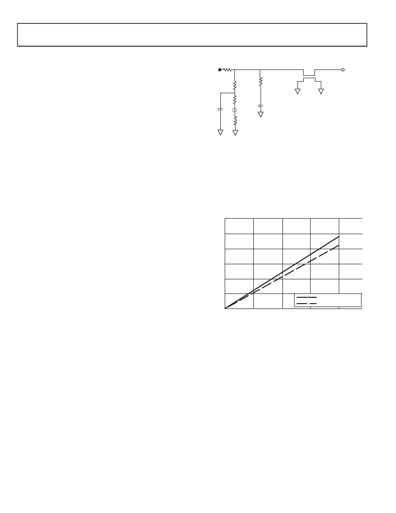
�Figure� 60.� Equivalent� Device� Loading� for� AC� Measurements�
�(Includes� All� Fixtures)�
�12�
�10�
�t� RISE�
�8�
�t� FALL�
�6�
�4�
�Capacitive� Loading�
�Output� delays� and� holds� are� based� on� standard� capacitive� loads�
�of� an� average� of� 6� pF� on� all� balls� (see� Figure� 60� ).� V� LOAD� is� equal�
�2�
�0�
�t� RISE� =� 1.8V� @� 25� °C�
�t� FALL� =� 1.8V� @� 25� °C�
�to� (V� DDEXT� /V� DDMEM� )� /2.� The� graphs� of� Figure� 61� through�
�0�
�50�
�100�
�150�
�200�
��The� delay� and� hold� specifications� given� should� be� derated� by� a�
�factor� derived� from� these� figures.� The� graphs� in� these� figures�
�may� not� be� linear� outside� the� ranges� shown.�
�LOAD� CAPACITANCE� (pF)�
�Figure� 61.� Driver� Type� A� Typical� Rise� and� Fall� Times� (10%–90%)� vs.�
�Load� Capacitance� (1.8V� V� DDEXT� /V� DDMEM� )�
�Rev.� D�
�|�
�Page� 76� of� 88� |� July� 2013�
�相关PDF资料 |
PDF描述 |
|---|---|
| NMH0505SC | CONV DC/DC 2W 5VIN 5VOUT SIP DL |
| IRU1207-33CSTR | IC REG LDO 3.3V 1A 8-SOIC |
| ADSP-2191MKCAZ-160 | IC DSP CONTROLLER 16BIT 144MBGA |
| DRA73-100-R | INDUCTOR HI TEMP 10UH 2.11A SMD |
| ADSP-2191MBCAZ-140 | IC DSP CONTROLLER 16BIT 144MBGA |
相关代理商/技术参数 |
参数描述 |
|---|---|
| ADSP-BF526BBCZ3 | 制造商:Analog Devices 功能描述: |
| ADSP-BF526BBCZ-3A | 功能描述:EMBEDDED PROCESSOR, BLACKFIN RoHS:是 类别:集成电路 (IC) >> 嵌入式 - DSP(数字式信号处理器) 系列:Blackfin® 标准包装:2 系列:StarCore 类型:SC140 内核 接口:DSI,以太网,RS-232 时钟速率:400MHz 非易失内存:外部 芯片上RAM:1.436MB 电压 - 输入/输出:3.30V 电压 - 核心:1.20V 工作温度:-40°C ~ 105°C 安装类型:表面贴装 封装/外壳:431-BFBGA,FCBGA 供应商设备封装:431-FCPBGA(20x20) 包装:托盘 |
| ADSP-BF526BBCZ-3AX | 制造商:Analog Devices 功能描述:DSP 32BIT 300MHZ 208CSPBGA - Trays |
| ADSP-BF526BBCZ-4A | 功能描述:IC DSP CTRLR 400MHZ 208CSPBGA RoHS:是 类别:集成电路 (IC) >> 嵌入式 - DSP(数字式信号处理器) 系列:Blackfin® 标准包装:40 系列:TMS320DM64x, DaVinci™ 类型:定点 接口:I²C,McASP,McBSP 时钟速率:400MHz 非易失内存:外部 芯片上RAM:160kB 电压 - 输入/输出:3.30V 电压 - 核心:1.20V 工作温度:0°C ~ 90°C 安装类型:表面贴装 封装/外壳:548-BBGA,FCBGA 供应商设备封装:548-FCBGA(27x27) 包装:托盘 配用:TMDSDMK642-0E-ND - DEVELPER KIT W/NTSC CAMERA296-23038-ND - DSP STARTER KIT FOR TMS320C6416296-23059-ND - FLASHBURN PORTING KIT296-23058-ND - EVAL MODULE FOR DM642TMDSDMK642-ND - DEVELOPER KIT W/NTSC CAMERA |
| ADSP-BF526BBCZ-4AX | 制造商:Analog Devices 功能描述:DSP 32BIT 400MHZ 208CSPBGA - Trays |
发布紧急采购,3分钟左右您将得到回复。