- 您现在的位置:买卖IC网 > PDF目录16699 > AFE7222EVM (Texas Instruments)EVAL MODULE FOR AFE7222 PDF资料下载
参数资料
| 型号: | AFE7222EVM |
| 厂商: | Texas Instruments |
| 文件页数: | 98/106页 |
| 文件大小: | 0K |
| 描述: | EVAL MODULE FOR AFE7222 |
| 标准包装: | 1 |
| 主要目的: | 接口,模拟前端(AFE) |
| 嵌入式: | 否 |
| 已用 IC / 零件: | AFE7222 |
| 已供物品: | 板 |
| 其它名称: | 296-30300 AFE7222EVM-ND |
第1页第2页第3页第4页第5页第6页第7页第8页第9页第10页第11页第12页第13页第14页第15页第16页第17页第18页第19页第20页第21页第22页第23页第24页第25页第26页第27页第28页第29页第30页第31页第32页第33页第34页第35页第36页第37页第38页第39页第40页第41页第42页第43页第44页第45页第46页第47页第48页第49页第50页第51页第52页第53页第54页第55页第56页第57页第58页第59页第60页第61页第62页第63页第64页第65页第66页第67页第68页第69页第70页第71页第72页第73页第74页第75页第76页第77页第78页第79页第80页第81页第82页第83页第84页第85页第86页第87页第88页第89页第90页第91页第92页第93页第94页第95页第96页第97页当前第98页第99页第100页第101页第102页第103页第104页第105页第106页
TO GET INTO DIRECT ACCESS
MODE
SDATA
SCLK
SEN
AUX DAC A INPUT1
0
1
0
1
DA11 DA10
DA9
DA8
DA7
DA6
DA5
DA4
DA3
DA2
DA1
DA0
AUX DAC B INPUT1
DB10
DB9
DB8
DB7
DB6
DB5
DB4
DB3
DB2
DB1
DB0
DB11
SDOUT
AUXDAC_A
AUXDAC_B
DELAY FOR FIRST UPDATE = 22 CLOCKS
DA10
DA9
DA8
DA7
DA6
DA5
DA4
DA3
DA2
DA1
DA0
DB10
DB9
DB8
DB7
DB6
DB5
DB4
DB3
DB2
DB1
DA11
DB11
DB0
DA10
DA9
DA8
DA7
DA6
DA5
DA4
DB10
DB9
DB8
DB7
DB6
DB5
DB4
DB11
DA11
DELAY FOR SUBSEQUENT UPDATE = 12 CLOCKS
AUX DAC A INPUT2
AUX DAC B INPUT2
tPER
tSETTLE
SLOS711B – NOVEMBER 2011 – REVISED MARCH 2012
AUXDAC_A_N is the internal complementary node and has an internal resistor, RINT programmable from
57 Ohm to 400 Ohm (using bits AUX_DAC_TERM_N<2:0>). For best linearity, choose a value of this
resistor to be as close to REXT as possible.
10.10 Enabling the Auxiliary DAC
The Auxiliary DACs are disabled by default.
Note that address of the 20 bit serial interface write bus is the 1st 12 bits out of which the 1st 4 bits
determine the access mode for the Auxiliary DAC.
Let us denote this address as ADDR<11:0>.
Following are Aux DAC modes:
If ADDR<11:8> = 0100, then we enter Direct Access mode for DAC. In this mode, DAC data is
dynamically written through SDATA (and SDOUT).
If ADDR<11:8> = 0101, then we enter the Register Access mode. In this mode, DAC is loaded with the
data from contents of pre-loaded registers.
In direct access mode
If ADDR<7:6> = 01: DAC_A will get written with the 12 serial bits from SDATA, DAC_B will get written
with the 12 serial bits from SDOUT (both at the rising edge of SCLK)
If ADDR<7:6> = 10: DAC_A will get 12 bits from SDATA, DAC_B will get next 12 bits from SDATA
(both at the rising edge of SCLK)
If ADDR<7:6> = 11: DAC_A will get 12 bits from SDATA at the rising edge of SCLK, DAC_B will get 12
bits from SDATA at the falling edge of SCLK.
In register access mode:
ADDR<7:6> = 01: Only DAC_A will be loaded with the register
ADDR<7:6> = 10: Only DAC_B will be loaded
ADDR<7:6> = 11: Both DAC_A and DAC_B are loaded.
For either direct access or register access modes, only the 1st 6 bits of the address need to be written for
the serial interface state machine. Remainig bits are considered as applicable to the DAC data.
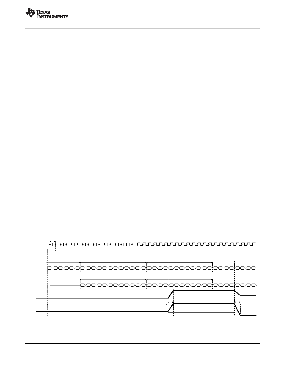
Below diagram shows the Aux DAC timing for the direct access mode where DAC_A is written through
SDATA and DAC_B through SDOUT.
Start by already setting EN_AUXDACA and EN_AUXDACB bits high.
Figure 10-18. Aux DAC Timing Diagram: DAC_A is Written Through SDATA and DAC_B Through SDOUT
tPER = SCLK period > 25 ns
tSETTLE = Settling time of Aux DAC for full scale output (0-1.5V) = 40 ns
Copyright 2011–2012, Texas Instruments Incorporated
DIGITAL INTERFACE
91
相关PDF资料 |
PDF描述 |
|---|---|
| ECE-V1EA100NP | CAP ALUM 10UF 25V 20% SMD |
| 0210491116 | CABLE JUMPER 1.25MM .305M 39POS |
| UPM1J270MED1TD | CAP ALUM 27UF 63V 20% RADIAL |
| RNF-100-1-1/4-RD-SP | HEAT SHRINK TUBING |
| RNF-100-1-1/4-BU-SP | HEAT SHRINK TUBING |
相关代理商/技术参数 |
参数描述 |
|---|---|
| AFE7222IRGC25 | 功能描述:射频前端 Dual 12B,65MSPS ADC RoHS:否 制造商:Skyworks Solutions, Inc. 类型: 工作频率:2.4 GHz, 5 GHz 最大数据速率:54 Mbps 噪声系数: 工作电源电压:3.3 V 电源电流:180 mA 最大工作温度:+ 85 C 安装风格:SMD/SMT 封装 / 箱体:QFN-32 |
| AFE7222IRGCR | 功能描述:射频前端 Dual 12B,65MSPS ADC RoHS:否 制造商:Skyworks Solutions, Inc. 类型: 工作频率:2.4 GHz, 5 GHz 最大数据速率:54 Mbps 噪声系数: 工作电源电压:3.3 V 电源电流:180 mA 最大工作温度:+ 85 C 安装风格:SMD/SMT 封装 / 箱体:QFN-32 |
| AFE7222IRGCT | 功能描述:射频前端 Dual 12B,65MSPS ADC RoHS:否 制造商:Skyworks Solutions, Inc. 类型: 工作频率:2.4 GHz, 5 GHz 最大数据速率:54 Mbps 噪声系数: 工作电源电压:3.3 V 电源电流:180 mA 最大工作温度:+ 85 C 安装风格:SMD/SMT 封装 / 箱体:QFN-32 |
| AFE7225 | 制造商:TI 制造商全称:Texas Instruments 功能描述:Analog Front End Wideband Mixed-Signal Transceiver |
| AFE7225EVM | 功能描述:射频开发工具 AFE7225 Eval Mod RoHS:否 制造商:Taiyo Yuden 产品:Wireless Modules 类型:Wireless Audio 工具用于评估:WYSAAVDX7 频率: 工作电源电压:3.4 V to 5.5 V |
发布紧急采购,3分钟左右您将得到回复。