- 您现在的位置:买卖IC网 > PDF目录223348 > Am29LV400T-90RWAEB (Advanced Micro Devices, Inc.) 4 Megabit (512 K x 8-Bit/256 K x 16-Bit) CMOS 3.0 Volt-only Boot Sector Flash Memory PDF资料下载
参数资料
| 型号: | Am29LV400T-90RWAEB |
| 厂商: | Advanced Micro Devices, Inc. |
| 英文描述: | 4 Megabit (512 K x 8-Bit/256 K x 16-Bit) CMOS 3.0 Volt-only Boot Sector Flash Memory |
| 中文描述: | 4兆位(512亩x 8-Bit/256亩x 16位),3.0伏的CMOS只引导扇区闪存 |
| 文件页数: | 39/40页 |
| 文件大小: | 516K |
| 代理商: | AM29LV400T-90RWAEB |
第1页第2页第3页第4页第5页第6页第7页第8页第9页第10页第11页第12页第13页第14页第15页第16页第17页第18页第19页第20页第21页第22页第23页第24页第25页第26页第27页第28页第29页第30页第31页第32页第33页第34页第35页第36页第37页第38页当前第39页第40页
Am29LV400
8
PREL I M I N AR Y
DEVICE BUS OPERATIONS
This section describes the requirements and use of the
device bus operations, which are initiated through the
internal command register. The command register itself
does not occupy any addressable memory location.
The register is composed of latches that store the com-
mands, along with the address and data information
needed to execute the command. The contents of the
register serve as inputs to the internal state machine.
The state machine outputs dictate the function of the
device. Table 1 lists the device bus operations, the in-
puts and control levels they require, and the resulting
output. The following subsections describe each of
these operations in further detail.
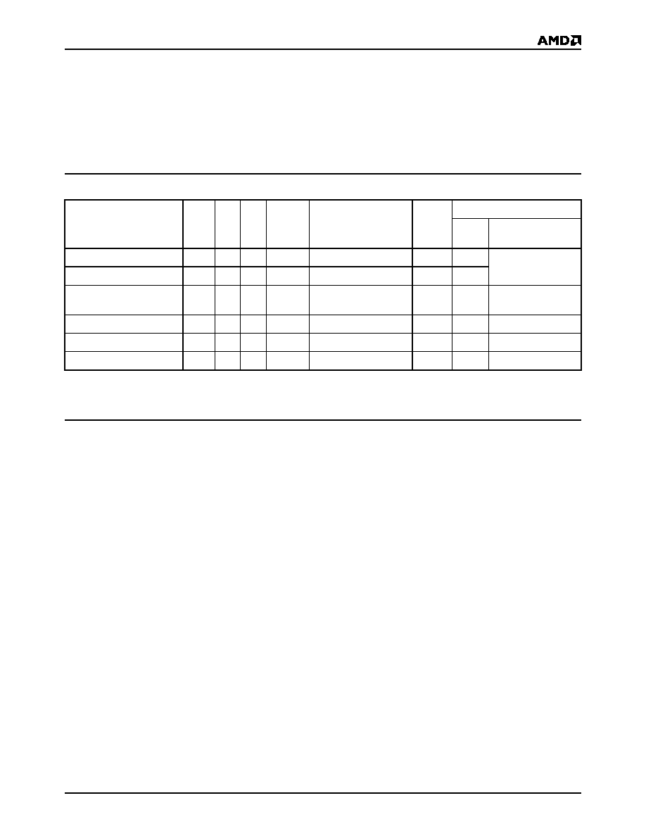
Table 1.
Am29LV400 Device Bus Operations
Legend:
L = Logic Low = VIL, H = Logic High = VIH, VID = 12.0 ± 0.5 V, X = Don’t Care, AIN = Addresses In, DIN = Data In, DOUT = Data Out
Note: Addresses are A17:A0 in word mode (BYTE# = VIH), A17:A-1 in byte mode (BYTE# = VIL).
Word/Byte Configuration
The BYTE# pin controls whether the device data I/O
pins DQ15–DQ0 operate in the byte or word configura-
tion. If the BYTE# pin is set at logic ‘1’, the device is in
word configuration, DQ15–DQ0 are active and control-
led by CE# and OE#.
If the BYTE# pin is set at logic ‘0’, the device is in byte
configuration, and only data I/O pins DQ0–DQ7 are ac-
tive and controlled by CE# and OE#. The data I/O pins
DQ8–DQ14 are tri-stated, and the DQ15 pin is used as
an input for the LSB (A-1) address function.
Requirements for Reading Array Data
To read array data from the outputs, the system must
drive the CE# and OE# pins to VIL. CE# is the power
control and selects the device. OE# is the output con-
trol and gates array data to the output pins. WE#
should remain at VIH. The BYTE# pin determines
whether the device outputs array data in words or
bytes.
The internal state machine is set for reading array data
upon device power-up, or after a hardware reset. This
ensures that no spurious alteration of the memory con-
tent occurs during the power transition. No command is
necessary in this mode to obtain array data. Standard
microprocessor read cycles that assert valid addresses
on the device address inputs produce valid data on the
device data outputs. The device remains enabled for
read access until the command register contents are
altered.
See “Reading Array Data” for more information. Refer
to the AC Read Operations table for timing specifica-
the DC Characteristics table represents the active cur-
rent specification for reading array data.
Writing Commands/Command Sequences
To write a command or command sequence (which in-
cludes programming data to the device and erasing
sectors of memory), the system must drive WE# and
CE# to VIL, and OE# to VIH.
For program operations, the BYTE# pin determines
whether the device accepts program data in bytes or
words. Refer to “Word/Byte Configuration” for more in-
formation.
An erase operation can erase one sector, multiple sec-
address space that each sector occupies. A “sector ad-
dress” consists of the address bits required to uniquely
select a sector. The “Command Definitions” section
Operation
CE#
OE# WE# RESET#
Addresses
DQ0–
DQ7
DQ8–DQ15
BYTE#
= VIH
BYTE#
= VIL
Read
L
H
AIN
DOUT
DOUT DQ8–DQ14 = High-Z,
DQ15 = A-1
Write
L
H
L
H
AIN
DIN
Standby
VCC ±
0.3 V
XX
VCC ±
0.3 V
X
High-Z
Output Disable
L
H
X
High-Z
Reset
X
L
X
High-Z
Temporary Sector Unprotect
X
VID
AIN
DIN
High-Z
相关PDF资料 |
PDF描述 |
|---|---|
| AM29LV400T-90RWAC | Ceramic Multilayer Capacitor; Capacitance:100pF; Capacitance Tolerance:+50, -20 %; Working Voltage, DC:100V; Dielectric Characteristic:NP0; Package/Case:1206; Series:W3F; Leaded Process Compatible:Yes |
| AM29LV400B-90RWAC | 4 Megabit (512 K x 8-Bit/256 K x 16-Bit) CMOS 3.0 Volt-only Boot Sector Flash Memory |
| Am29LV640DH90RZE | 8 Characters x 2 Lines, 5x7 Dot Matrix Character and Cursor |
| Am29LV640DL90RZE | 8 Characters x 2 Lines, 5x7 Dot Matrix Character and Cursor |
| Am29LV641DH90RZE | 8 Characters x 2 Lines, 5x7 Dot Matrix Character and Cursor |
相关代理商/技术参数 |
参数描述 |
|---|---|
| AM29LV640DH90REI | 制造商:Spansion 功能描述:FLASH PARALLEL 3V/3.3V 64MBIT 4MX16 90NS 48TSOP - Trays |
| AM29LV640DL90RZI | 制造商:Advanced Micro Devices 功能描述: |
| AM29LV640DU-90NI | 制造商:Advanced Micro Devices 功能描述: |
| AM29LV640DU90REI | 制造商:Spansion 功能描述:FLASH PARALLEL 3V/3.3V 64MBIT 4MX16 90NS 48TSOP - Trays |
| AM29LV640DU-90RWHIT | 制造商:Advanced Micro Devices 功能描述:63-BALL FINE-PITCH BALL GRID ARRAY (FBGA) 0.80 MM PITCH, 11 X 12 MM PACKAGE (FBE063) |
发布紧急采购,3分钟左右您将得到回复。