- 您现在的位置:买卖IC网 > PDF目录166232 > AS5SS256K36ADQ-8.5/883C (AUSTIN SEMICONDUCTOR INC) 256K x 36 SSRAM Flow-Through, Synchronous Burst SRAM PDF资料下载
参数资料
| 型号: | AS5SS256K36ADQ-8.5/883C |
| 厂商: | AUSTIN SEMICONDUCTOR INC |
| 元件分类: | SRAM |
| 英文描述: | 256K x 36 SSRAM Flow-Through, Synchronous Burst SRAM |
| 中文描述: | 256K X 36 STANDARD SRAM, 8.5 ns, PQFP100 |
| 封装: | 14 X 20 MM, 1.40 MM HEIGHT, MS-026, TQFP-100 |
| 文件页数: | 9/16页 |
| 文件大小: | 391K |
| 代理商: | AS5SS256K36ADQ-8.5/883C |
SSRAM
AS5SS256K36 &
AS5SS256K36A
AS5SS256K36 &
AS5SS256K36A
Rev. 3.6 06/05
Austin Semiconductor, Inc. reserves the right to change products or specifications without notice.
2
Austin Semiconductor, Inc.
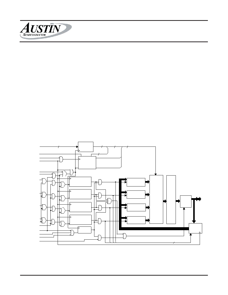
GENERAL DESCRIPTION (continued)
Asynchronous inputs include the output enable (OE\),
clock (CLK) and snooze enable (ZZ). There is also a burst
mode input (MODE) that selects between interleaved and lin-
ear burst modes. The data-out (Q), enabled by OE\, is also
asynchronous. WRITE cycles can be from one to four bytes
wide as controlled by the write control inputs.
Burst operation can be initiated with either address
status processor (ADSP\) or address status controller (ADSC\)
inputs. Subsequent burst addresses can be internally gener-
ated as controlled by the burst advance input (ADV\).
Address and write control are registered on-chip to
simplify WRITE cycles. This allows self-timed WRITE cycles.
Individual byte enables allow individual bytes to be written.
During WRITE cycles on the x18 device, BWa\ controls DQa’s
and DQPa; BWb\ controls DQb’s and DQPb; BWc\ controls
DQc’s and DQPc; BWd\ controls DQd’s and DQPd. GW\ LOW
causes all bytes to be written. Parity bits are also featured on
this device.
This 8Mb Synchronous Burst SRAM operates from a
+3.3V V
DD
power supply, and all inputs and outputs are TTL-
compatible. The device is ideally suited for 486, Pentium, 680x0
and PowerPCTM systems and those systems that benefit from a
wide synchronous data bus.
18
16
18
SA0, SA1, SAs
SA0-SA1
MODE
ADV\
CLK
SA1'
SA0'
BWd\
BWc\
DQs
DQPa
DQPb
DQPc
BWb\
DQPd
BWa\
BWE\
GW\
OE\
ADDRESS
REGISTER
BINARY
COUNTER
AND LOGIC
Q1
Q0
CL
ADSC\
ADSP\
BYTE "d"
WRITE REGISTER
BYTE "c"
WRITE REGISTER
BYTE "b"
WRITE REGISTER
BYTE "a"
WRITE REGISTER
ENABLE
REGISTER
CE\
CE2
CE2\
BYTE "d"
WRITE DRIVER
BYTE "c"
WRITE DRIVER
BYTE "b"
WRITE DRIVER
BYTE "a"
WRITE DRIVER
256K x 9 x 4
(x36)
MEMORY
ARRAY
SENSE
AMPS
OUTPUT
BUFFERS
INPUT
REGISTERS
4
FUNCTIONAL BLOCK DIAGRAM
NOTE: Functional Block Diagrams illustrate simplified device operation. See Truth Table, Pin Descriptions and time diagrams for detailed
information.
相关PDF资料 |
PDF描述 |
|---|---|
| AS6054 | 1000 MHz - 6000 MHz RF/MICROWAVE WIDE BAND LOW POWER AMPLIFIER |
| AS7C1028-15JC | 256K X 4 STANDARD SRAM, 15 ns, PDSO28 |
| AS7C25512FT32A-85BIN | 512K X 32 STANDARD SRAM, 8.5 ns, PBGA165 |
| AS7C25512NTD32A-166TQI | 512K X 32 ZBT SRAM, 3.5 ns, PQFP100 |
| AS7C3256K18Z-3.5TQC | 256K X 18 STANDARD SRAM, 3.5 ns, PQFP100 |
相关代理商/技术参数 |
参数描述 |
|---|---|
| AS5SS256K36DQ10 | 制造商:ASI 功能描述:NEW |
| AS5SS256K36DQ-10/883C | 制造商:AUSTIN 制造商全称:Austin Semiconductor 功能描述:256K x 36 SSRAM Flow-Through, Synchronous Burst SRAM |
| AS5SS256K36DQ-10/IT | 制造商:Micross Components 功能描述:SSRAM-FT, 9.0MB - Trays |
| AS5SS256K36DQ-10/XT | 制造商:AUSTIN 制造商全称:Austin Semiconductor 功能描述:256K x 36 SSRAM Flow-Through, Synchronous Burst SRAM |
| AS5SS256K36DQ-8.5/883C | 制造商:AUSTIN 制造商全称:Austin Semiconductor 功能描述:256K x 36 SSRAM Flow-Through, Synchronous Burst SRAM |
发布紧急采购,3分钟左右您将得到回复。