- 您现在的位置:买卖IC网 > PDF目录20402 > AT25DF321-S3U (Atmel)IC FLASH 32MBIT 70MHZ 16SOIC PDF资料下载
参数资料
| 型号: | AT25DF321-S3U |
| 厂商: | Atmel |
| 文件页数: | 3/37页 |
| 文件大小: | 0K |
| 描述: | IC FLASH 32MBIT 70MHZ 16SOIC |
| 标准包装: | 46 |
| 格式 - 存储器: | 闪存 |
| 存储器类型: | DataFLASH |
| 存储容量: | 32M(16384 页 x 256 字节) |
| 速度: | 70MHz |
| 接口: | SPI 3 线串行 |
| 电源电压: | 2.7 V ~ 3.6 V |
| 工作温度: | -40°C ~ 85°C |
| 封装/外壳: | 16-SOIC(0.295",7.50mm 宽) |
| 供应商设备封装: | 16-SOIC |
| 包装: | 管件 |
第1页第2页当前第3页第4页第5页第6页第7页第8页第9页第10页第11页第12页第13页第14页第15页第16页第17页第18页第19页第20页第21页第22页第23页第24页第25页第26页第27页第28页第29页第30页第31页第32页第33页第34页第35页第36页第37页
�� �
�
�AT25DF321�
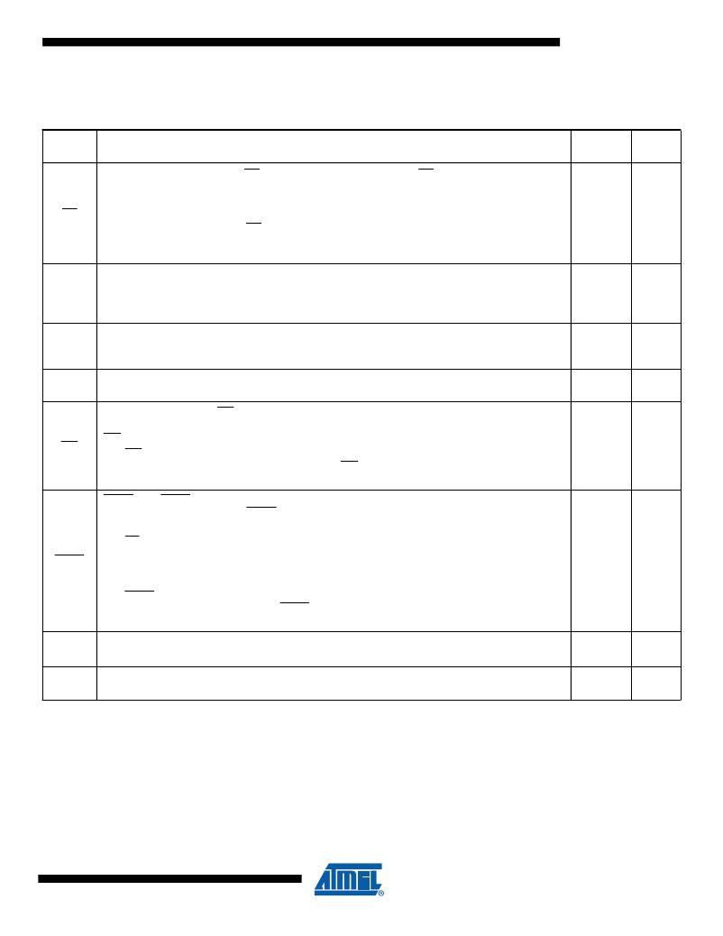
�2.� Pin� Descriptions� and� Pinouts�
�Table� 2-1.�
�Pin� Descriptions�
�Asserted�
�Symbol�
�Name� and� Function�
�State�
�Type�
�CHIP� SELECT� :� Asserting� the� CS� pin� selects� the� device.� When� the� CS� pin� is� deasserted,� the�
�device� will� be� deselected� and� normally� be� placed� in� standby� mode� (not� Deep� Power-Down� mode),�
�and� the� SO� pin� will� be� in� a� high-impedance� state.� When� the� device� is� deselected,� data� will� not� be�
�CS�
�accepted� on� the� SI� pin.�
�Low�
�Input�
�A� high-to-low� transition� on� the� CS� pin� is� required� to� start� an� operation,� and� a� low-to-high� transition�
�is� required� to� end� an� operation.� When� ending� an� internally� self-timed� operation� such� as� a� program�
�or� erase� cycle,� the� device� will� not� enter� the� standby� mode� until� the� completion� of� the� operation.�
�SERIAL� CLOCK� :� This� pin� is� used� to� provide� a� clock� to� the� device� and� is� used� to� control� the� flow� of�
�SCK�
�SI�
�SO�
�data� to� and� from� the� device.� Command,� address,� and� input� data� present� on� the� SI� pin� is� always�
�latched� on� the� rising� edge� of� SCK,� while� output� data� on� the� SO� pin� is� always� clocked� out� on� the�
�falling� edge� of� SCK.�
�SERIAL� INPUT� :� The� SI� pin� is� used� to� shift� data� into� the� device.� The� SI� pin� is� used� for� all� data� input�
�including� command� and� address� sequences.� Data� on� the� SI� pin� is� always� latched� on� the� rising�
�edge� of� SCK.�
�SERIAL� OUTPUT� :� The� SO� pin� is� used� to� shift� data� out� from� the� device.� Data� on� the� SO� pin� is�
�always� clocked� out� on� the� falling� edge� of� SCK.�
�WRITE� PROTECT� :� The� WP� pin� controls� the� hardware� locking� feature� of� the� device.� Please� refer� to�
�“Protection� Commands� and� Features”� on� page� 12� for� more� details� on� protection� features� and� the�
�Input�
�Input�
�Output�
�WP�
�WP� pin.�
�The� WP� pin� is� internally� pulled-high� and� may� be� left� floating� if� hardware� controlled� protection� will�
�Low�
�Input�
�not� be� used.� However,� it� is� recommended� that� the� WP� pin� also� be� externally� connected� to� V� CC�
�whenever� possible.�
�HOLD� :� The� HOLD� pin� is� used� to� temporarily� pause� serial� communication� without� deselecting� or�
�resetting� the� device.� While� the� HOLD� pin� is� asserted,� transitions� on� the� SCK� pin� and� data� on� the� SI�
�pin� will� be� ignored,� and� the� SO� pin� will� be� in� a� high-impedance� state.�
�The� CS� pin� must� be� asserted,� and� the� SCK� pin� must� be� in� the� low� state� in� order� for� a� Hold�
�HOLD�
�condition� to� start.� A� Hold� condition� pauses� serial� communication� only� and� does� not� have� an� effect�
�on� internally� self-timed� operations� such� as� a� program� or� erase� cycle.� Please� refer� to� “Hold”� on�
�Low�
�Input�
�page� 27� for� additional� details� on� the� Hold� operation.�
�The� HOLD� pin� is� internally� pulled-high� and� may� be� left� floating� if� the� Hold� function� will� not� be� used.�
�However,� it� is� recommended� that� the� HOLD� pin� also� be� externally� connected� to� V� CC� whenever�
�possible.�
�V� CC�
�GND�
�DEVICE� POWER� SUPPLY� :� The� V� CC� pin� is� used� to� supply� the� source� voltage� to� the� device.�
�Operations� at� invalid� V� CC� voltages� may� produce� spurious� results� and� should� not� be� attempted.�
�GROUND� :� The� ground� reference� for� the� power� supply.� GND� should� be� connected� to� the� system�
�ground.�
�Power�
�Power�
�3�
�3669B–DFLASH–6/09�
�相关PDF资料 |
PDF描述 |
|---|---|
| IR2111S | IC DRIVER HALF-BRIDGE 8-SOIC |
| 346-080-522-802 | CARDEDGE 80POS DUAL .125 GREEN |
| AT24C512BN-SH-B | IC EEPROM 512KBIT 1MHZ 8SOIC |
| MLG1005SR30J | INDUCTOR MULTILAYER .30UH 0402 |
| IR2110STR | IC DRIVER HIGH/LOW SIDE 16-SOIC |
相关代理商/技术参数 |
参数描述 |
|---|---|
| AT25DF321-SU | 功能描述:闪存 32 Megabit 2.7V RoHS:否 制造商:ON Semiconductor 数据总线宽度:1 bit 存储类型:Flash 存储容量:2 MB 结构:256 K x 8 定时类型: 接口类型:SPI 访问时间: 电源电压-最大:3.6 V 电源电压-最小:2.3 V 最大工作电流:15 mA 工作温度:- 40 C to + 85 C 安装风格:SMD/SMT 封装 / 箱体: 封装:Reel |
| AT25DF512C-MAHNGU-T | 功能描述:IC FLASH 512KB 8UDFN 制造商:adesto technologies 系列:- 包装:带卷(TR) 零件状态:有效 格式 - 存储器:闪存 存储器类型:FLASH 存储容量:512K(64K x 8) 速度:85MHz 接口:SPI 串行 电压 - 电源:1.65 V ~ 3.6 V 工作温度:-40°C ~ 85°C(TC) 封装/外壳:8-UFDFN 裸露焊盘 供应商器件封装:8-UDFN(2x3) 标准包装:5,000 |
| AT25DF512C-MAHNGU-Y | 功能描述:IC FLASH 512KB 8UDFN 制造商:adesto technologies 系列:- 包装:托盘 零件状态:停产 格式 - 存储器:闪存 存储器类型:FLASH 存储容量:512K(64K x 8) 速度:85MHz 接口:SPI 串行 电压 - 电源:1.65 V ~ 3.6 V 工作温度:-40°C ~ 85°C(TC) 封装/外壳:8-UFDFN 裸露焊盘 供应商器件封装:8-UDFN(2x3) 标准包装:490 |
| AT25DF512C-MAHN-T | 功能描述:IC FLASH 512KB 8UDFN 制造商:adesto technologies 系列:- 包装:剪切带(CT) 零件状态:有效 格式 - 存储器:闪存 存储器类型:FLASH 存储容量:512K(64K x 8) 速度:85MHz 接口:SPI 串行 电压 - 电源:1.65 V ~ 3.6 V 工作温度:-40°C ~ 85°C(TC) 封装/外壳:8-UFDFN 裸露焊盘 供应商器件封装:8-UDFN(2x3) 标准包装:1 |
| AT25DF512C-MAHN-Y | 功能描述:IC FLASH 512KB 8UDFN 制造商:adesto technologies 系列:- 包装:托盘 零件状态:停产 格式 - 存储器:闪存 存储器类型:FLASH 存储容量:512K(64K x 8) 速度:85MHz 接口:SPI 串行 电压 - 电源:1.65 V ~ 3.6 V 工作温度:-40°C ~ 85°C(TC) 封装/外壳:8-UFDFN 裸露焊盘 供应商器件封装:8-UDFN(2x3) 标准包装:490 |
发布紧急采购,3分钟左右您将得到回复。