- 您现在的位置:买卖IC网 > PDF目录381463 > AT49BV8011T (Atmel Corp.) 8-megabit 3-volt Flash Memory(8M位 3V闪速存储器) PDF资料下载
参数资料
| 型号: | AT49BV8011T |
| 厂商: | Atmel Corp. |
| 英文描述: | 8-megabit 3-volt Flash Memory(8M位 3V闪速存储器) |
| 中文描述: | 8兆位3伏的快闪记忆体(800万位3V的闪速存储器) |
| 文件页数: | 6/18页 |
| 文件大小: | 322K |
| 代理商: | AT49BV8011T |
AT49BV/LV8011(T)
6
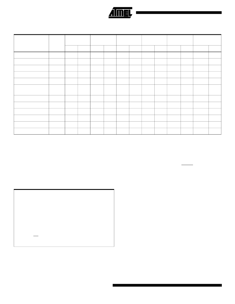
Notes:
1. The DATA FORMAT in each bus cycle is as follows: I/O15 - I/O8 (Don
’
t Care); I/O7 - I/O0 (Hex).
The ADDRESS FORMAT in each bus cycle is as follows: A15 - A0 (Hex). Address A18 through A14 are Don
’
t Care in the
word mode. Address A18 through A14 and A-1 are Don
’
t Care in the byte mode.
2. Either one of the Product ID Exit commands can be used.
3. SA = sector address. Any byte/word address within a sector can be used to designate the sector address (see next two
pages for details).
4. When the sector programming lockout feature is not enabled, the sector will erase (from the same Sector Erase command).
Once the sector has been protected, data in the protected sectors cannot be changed unless the RESET pin is taken to
12V ± 0.5V.
5. PA is the plane address (A18 - A16).
Command Definition in (Hex)
(1)
Command
Sequence
Bus
Cycles
1st Bus
Cycle
2nd Bus
Cycle
3rd Bus
Cycle
4th Bus
Cycle
5th Bus
Cycle
6th Bus
Cycle
Addr
Data
Addr
Data
Addr
Data
Addr
Data
Addr
Data
Addr
Data
Read
1
Addr
D
OUT
Chip Erase
6
5555
AA
2AAA
55
5555
80
5555
AA
2AAA
55
5555
10
Sector Erase
6
5555
AA
2AAA
55
5555
80
5555
AA
2AAA
55
SA
(3)(4)
30
Byte/Word Program
4
5555
AA
2AAA
55
5555
A0
Addr
D
IN
Bypass Unlock
6
5555
AA
2AAA
55
5555
80
5555
AA
2AAA
55
5555
A0
Single-pulse
Byte/Word Program
1
Addr
D
IN
Sector Lockout
6
5555
AA
2AAA
55
5555
80
5555
AA
2AAA
55
SA
(3)(4)
40
Erase Suspend
1
xxxx
B0
Erase Resume
1
PA
(5)
30
Product ID Entry
3
5555
AA
2AAA
55
5555
90
Product ID Exit
(2)
3
5555
AA
2AAA
55
5555
F0
Product ID Exit
(2)
1
xxxx
F0
Absolute Maximum Ratings*
Temperature under Bias ................................ -55
°
C to +125
°
C
*NOTICE:
Stresses beyond those listed under
“
Absolute
Maximum Ratings
”
may cause permanent dam-
age to the device. This is a stress rating only and
functional operation of the device at these or any
other conditions beyond those indicated in the
operational sections of this specification is not
implied. Exposure to absolute maximum rating
conditions for extended periods may affect device
reliability.
Storage Temperature..................................... -65
°
C to +150
°
C
All Input Voltages
(including NC Pins)
with Respect to Ground...................................-0.6V to +6.25V
All Output Voltages
with Respect to Ground.............................-0.6V to V
CC
+ 0.6V
Voltage on OE
with Respect to Ground...................................-0.6V to +13.5V
相关PDF资料 |
PDF描述 |
|---|---|
| AT49LV8011 | 8-megabit 3-volt Flash Memory(8M位 3V闪速存储器) |
| AT49LV8011T | 8-megabit 3-volt Flash Memory(8M位 3V闪速存储器) |
| AT49BV802A | 8-megabit (512K x 16/ 1M x 8) 3-volt Only Flash Memory |
| AT49BV802A-70CI | 8-megabit (512K x 16/ 1M x 8) 3-volt Only Flash Memory |
| AT49BV802A-70TI | 8-megabit (512K x 16/ 1M x 8) 3-volt Only Flash Memory |
相关代理商/技术参数 |
参数描述 |
|---|---|
| AT49BV8011T-12CC | 制造商:未知厂家 制造商全称:未知厂家 功能描述:x8/x16 Flash EEPROM |
| AT49BV8011T-12CI | 制造商:未知厂家 制造商全称:未知厂家 功能描述:x8/x16 Flash EEPROM |
| AT49BV8011T-12TC | 制造商:未知厂家 制造商全称:未知厂家 功能描述:x8/x16 Flash EEPROM |
| AT49BV8011T-12TI | 制造商:ATMEL 制造商全称:ATMEL Corporation 功能描述:8-megabit (512K x 16/1M x 8) 3-volt Only Flash Memory |
| AT49BV8011T-90CC | 制造商:未知厂家 制造商全称:未知厂家 功能描述:x8/x16 Flash EEPROM |
发布紧急采购,3分钟左右您将得到回复。