- 您现在的位置:买卖IC网 > PDF目录12052 > AT89LP3240-20PU (Atmel)MCU 8051 32K FLASH 20MHZ PDF资料下载
参数资料
| 型号: | AT89LP3240-20PU |
| 厂商: | Atmel |
| 文件页数: | 186/200页 |
| 文件大小: | 0K |
| 描述: | MCU 8051 32K FLASH 20MHZ |
| 标准包装: | 10 |
| 系列: | 89LP |
| 核心处理器: | 8051 |
| 芯体尺寸: | 8-位 |
| 速度: | 20MHz |
| 连通性: | I²C,SPI,UART/USART |
| 外围设备: | 欠压检测/复位,POR,PWM,WDT |
| 输入/输出数: | 38 |
| 程序存储器容量: | 32KB(32K x 8) |
| 程序存储器类型: | 闪存 |
| EEPROM 大小: | 8K x 8 |
| RAM 容量: | 4.25K x 8 |
| 电压 - 电源 (Vcc/Vdd): | 2.4 V ~ 3.6 V |
| 数据转换器: | A/D 8x10b |
| 振荡器型: | 内部 |
| 工作温度: | -40°C ~ 85°C |
| 封装/外壳: | 40-DIP(0.540",13.72mm) |
| 包装: | 管件 |
第1页第2页第3页第4页第5页第6页第7页第8页第9页第10页第11页第12页第13页第14页第15页第16页第17页第18页第19页第20页第21页第22页第23页第24页第25页第26页第27页第28页第29页第30页第31页第32页第33页第34页第35页第36页第37页第38页第39页第40页第41页第42页第43页第44页第45页第46页第47页第48页第49页第50页第51页第52页第53页第54页第55页第56页第57页第58页第59页第60页第61页第62页第63页第64页第65页第66页第67页第68页第69页第70页第71页第72页第73页第74页第75页第76页第77页第78页第79页第80页第81页第82页第83页第84页第85页第86页第87页第88页第89页第90页第91页第92页第93页第94页第95页第96页第97页第98页第99页第100页第101页第102页第103页第104页第105页第106页第107页第108页第109页第110页第111页第112页第113页第114页第115页第116页第117页第118页第119页第120页第121页第122页第123页第124页第125页第126页第127页第128页第129页第130页第131页第132页第133页第134页第135页第136页第137页第138页第139页第140页第141页第142页第143页第144页第145页第146页第147页第148页第149页第150页第151页第152页第153页第154页第155页第156页第157页第158页第159页第160页第161页第162页第163页第164页第165页第166页第167页第168页第169页第170页第171页第172页第173页第174页第175页第176页第177页第178页第179页第180页第181页第182页第183页第184页第185页当前第186页第187页第188页第189页第190页第191页第192页第193页第194页第195页第196页第197页第198页第199页第200页
86
3706C–MICRO–2/11
AT89LP3240/6440
bit and prepares to receive the data bytes that follows. The slaves that are not addressed set
their SM2 bits and ignore the data bytes. See “Automatic Address Recognition” on page 97.
The SM2 bit can be used to check the validity of the stop bit in Mode 1. In a Mode 1 reception, if
SM2 = 1, the receive interrupt is not activated unless a valid stop bit is received.
Notes:1. SMOD0 is located at PCON.6.
2. f
osc = oscillator frequency. The baud rate depends on SMOD1 (PCON.7).
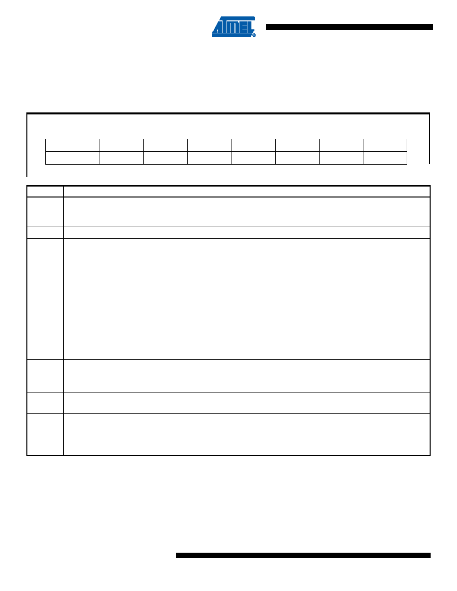
Table 16-1.
SCON – Serial Port Control Register
SCON Address = 98H
Reset Value = 0000 0000B
Bit Addressable
SM0/FE
SM1
SM2
REN
TB8
RB8
T1
RI
Bit
7
65
43
21
0
(SMOD0 = 0/1)(1)
Symbol
Function
FE
Framing error bit. This bit is set by the receiver when an invalid stop bit is detected. The FE bit is not cleared by valid
frames and must be cleared by software. The SMOD0 bit must be set to enable access to the FE bit. FE will be set
regardless of the state of SMOD0.
SM0
Serial Port Mode Bit 0, (SMOD0 must = 0 to access bit SM0)
SM1
Serial Port Mode Bit 1
SM2
Enables the Automatic Address Recognition feature in Modes 2 or 3. If SM2 = 1 then Rl will not be set unless the received
9th data bit (RB8) is 1, indicating an address, and the received byte is a Given or Broadcast Address. In Mode 1, if SM2 =
1 then Rl will not be activated unless a valid stop bit was received, and the received byte is a Given or Broadcast Address.
In Mode 0, SM2 determines the idle state of the shift clock such that the clock is the inverse of SM2, i.e. when SM2 = 0
the clock idles high and when SM2 = 1 the clock idles low.
REN
Enables serial reception. Set by software to enable reception. Clear by software to disable reception.
TB8
The 9th data bit that will be transmitted in Modes 2 and 3. Set or clear by software as desired. In Mode 0, setting TB8
enables Timer 1 as the shift clock generator.
RB8
In Modes 2 and 3, the 9th data bit that was received. In Mode 1, if SM2 = 0, RB8 is the stop bit that was received. In Mode
0, RB8 is not used.
TI
Transmit interrupt flag. Set by hardware at the end of the 8th bit time in Mode 0, or at the beginning of the stop bit in the
other modes, in any serial transmission. Must be cleared by software.
RI
Receive interrupt flag. Set by hardware at the end of the 8th bit time in Mode 0, or halfway through the stop bit time in the
other modes, in any serial reception (except see SM2). Must be cleared by software.
SM0
SM1
Mode
Description
Baud Rate(2)
000
shift register
f
osc/2 or fosc/4 or Timer 1
011
8-bit UART
variable (Timer 1 or Timer 2)
102
9-bit UART
f
osc/32 or fosc/16
113
9-bit UART
variable (Timer 1 or Timer 2)
相关PDF资料 |
PDF描述 |
|---|---|
| VI-JTZ-IY-F4 | CONVERTER MOD DC/DC 2V 20W |
| VI-JTZ-IY-F2 | CONVERTER MOD DC/DC 2V 20W |
| ATMEGA164A-PU | IC MCU AVR 16K 20MHZ 40PDIP |
| VI-J0J-IX-B1 | CONVERTER MOD DC/DC 36V 75W |
| VI-JTZ-IY-F1 | CONVERTER MOD DC/DC 2V 20W |
相关代理商/技术参数 |
参数描述 |
|---|---|
| AT89LP4052-16PI | 功能描述:8位微控制器 -MCU Microcontroller RoHS:否 制造商:Silicon Labs 核心:8051 处理器系列:C8051F39x 数据总线宽度:8 bit 最大时钟频率:50 MHz 程序存储器大小:16 KB 数据 RAM 大小:1 KB 片上 ADC:Yes 工作电源电压:1.8 V to 3.6 V 工作温度范围:- 40 C to + 105 C 封装 / 箱体:QFN-20 安装风格:SMD/SMT |
| AT89LP4052-16PU | 功能描述:8位微控制器 -MCU Microcontroller RoHS:否 制造商:Silicon Labs 核心:8051 处理器系列:C8051F39x 数据总线宽度:8 bit 最大时钟频率:50 MHz 程序存储器大小:16 KB 数据 RAM 大小:1 KB 片上 ADC:Yes 工作电源电压:1.8 V to 3.6 V 工作温度范围:- 40 C to + 105 C 封装 / 箱体:QFN-20 安装风格:SMD/SMT |
| AT89LP4052-16SI | 功能描述:8位微控制器 -MCU Microcontroller RoHS:否 制造商:Silicon Labs 核心:8051 处理器系列:C8051F39x 数据总线宽度:8 bit 最大时钟频率:50 MHz 程序存储器大小:16 KB 数据 RAM 大小:1 KB 片上 ADC:Yes 工作电源电压:1.8 V to 3.6 V 工作温度范围:- 40 C to + 105 C 封装 / 箱体:QFN-20 安装风格:SMD/SMT |
| AT89LP4052-16SU | 功能描述:IC 8051 MCU FLASH 4K 20SOIC RoHS:是 类别:集成电路 (IC) >> 嵌入式 - 微控制器, 系列:89LP 标准包装:1,500 系列:AVR® ATtiny 核心处理器:AVR 芯体尺寸:8-位 速度:16MHz 连通性:I²C,LIN,SPI,UART/USART,USI 外围设备:欠压检测/复位,POR,PWM,温度传感器,WDT 输入/输出数:16 程序存储器容量:8KB(4K x 16) 程序存储器类型:闪存 EEPROM 大小:512 x 8 RAM 容量:512 x 8 电压 - 电源 (Vcc/Vdd):2.7 V ~ 5.5 V 数据转换器:A/D 11x10b 振荡器型:内部 工作温度:-40°C ~ 125°C 封装/外壳:20-SOIC(0.295",7.50mm 宽) 包装:带卷 (TR) |
| AT89LP4052-16XI | 功能描述:8位微控制器 -MCU Microcontroller RoHS:否 制造商:Silicon Labs 核心:8051 处理器系列:C8051F39x 数据总线宽度:8 bit 最大时钟频率:50 MHz 程序存储器大小:16 KB 数据 RAM 大小:1 KB 片上 ADC:Yes 工作电源电压:1.8 V to 3.6 V 工作温度范围:- 40 C to + 105 C 封装 / 箱体:QFN-20 安装风格:SMD/SMT |
发布紧急采购,3分钟左右您将得到回复。