- 您现在的位置:买卖IC网 > PDF目录12052 > AT89LP3240-20PU (Atmel)MCU 8051 32K FLASH 20MHZ PDF资料下载
参数资料
| 型号: | AT89LP3240-20PU |
| 厂商: | Atmel |
| 文件页数: | 3/200页 |
| 文件大小: | 0K |
| 描述: | MCU 8051 32K FLASH 20MHZ |
| 标准包装: | 10 |
| 系列: | 89LP |
| 核心处理器: | 8051 |
| 芯体尺寸: | 8-位 |
| 速度: | 20MHz |
| 连通性: | I²C,SPI,UART/USART |
| 外围设备: | 欠压检测/复位,POR,PWM,WDT |
| 输入/输出数: | 38 |
| 程序存储器容量: | 32KB(32K x 8) |
| 程序存储器类型: | 闪存 |
| EEPROM 大小: | 8K x 8 |
| RAM 容量: | 4.25K x 8 |
| 电压 - 电源 (Vcc/Vdd): | 2.4 V ~ 3.6 V |
| 数据转换器: | A/D 8x10b |
| 振荡器型: | 内部 |
| 工作温度: | -40°C ~ 85°C |
| 封装/外壳: | 40-DIP(0.540",13.72mm) |
| 包装: | 管件 |
第1页第2页当前第3页第4页第5页第6页第7页第8页第9页第10页第11页第12页第13页第14页第15页第16页第17页第18页第19页第20页第21页第22页第23页第24页第25页第26页第27页第28页第29页第30页第31页第32页第33页第34页第35页第36页第37页第38页第39页第40页第41页第42页第43页第44页第45页第46页第47页第48页第49页第50页第51页第52页第53页第54页第55页第56页第57页第58页第59页第60页第61页第62页第63页第64页第65页第66页第67页第68页第69页第70页第71页第72页第73页第74页第75页第76页第77页第78页第79页第80页第81页第82页第83页第84页第85页第86页第87页第88页第89页第90页第91页第92页第93页第94页第95页第96页第97页第98页第99页第100页第101页第102页第103页第104页第105页第106页第107页第108页第109页第110页第111页第112页第113页第114页第115页第116页第117页第118页第119页第120页第121页第122页第123页第124页第125页第126页第127页第128页第129页第130页第131页第132页第133页第134页第135页第136页第137页第138页第139页第140页第141页第142页第143页第144页第145页第146页第147页第148页第149页第150页第151页第152页第153页第154页第155页第156页第157页第158页第159页第160页第161页第162页第163页第164页第165页第166页第167页第168页第169页第170页第171页第172页第173页第174页第175页第176页第177页第178页第179页第180页第181页第182页第183页第184页第185页第186页第187页第188页第189页第190页第191页第192页第193页第194页第195页第196页第197页第198页第199页第200页
100
3706C–MICRO–2/11
AT89LP3240/6440
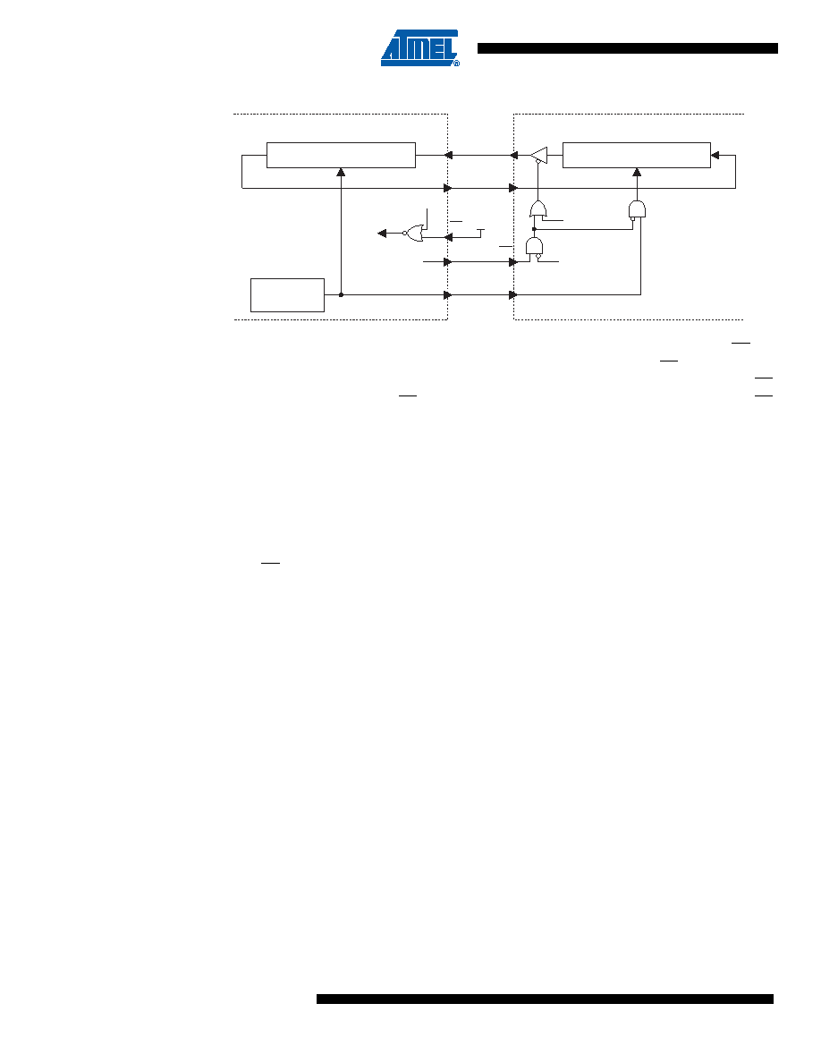
Figure 17-2. SPI Master-Slave Interconnection
When the SPI is configured as a Master (MSTR in SPCR is set), the operation of the SS pin
depends on the setting of the Slave Select Ignore bit, SSIG. If SSIG = 1, the SS pin is a general
purpose output pin which does not affect the SPI system. Typically, the pin will be driving the SS
pin of an SPI Slave. If SSIG = 0, SS must be held high to ensure Master SPI operation. If the SS
pin is driven low by peripheral circuitry when the SPI is configured as a Master with SSIG = 0,
the SPI system interprets this as another master selecting the SPI as a slave and starting to
send data to it. To avoid bus contention, the SPI system takes the following actions:
1.
The MSTR bit in SPCR is cleared and the SPI system becomes a Slave. As a result of
the SPI becoming a Slave, the MOSI and SCK pins become inputs.
2.
The MODF Flag in SPSR is set, and if the SPI interrupt is enabled, the interrupt routine
will be executed.
Thus, when interrupt-driven SPI transmission is used in Master mode, and there exists a possi-
bility that SS may be driven low, the interrupt should always check that the MSTR bit is still set. If
the MSTR bit has been cleared by a slave select, it must be set by the user to re-enable SPI
Master mode.
17.1
Master Operation
An SPI master device initiates all data transfers on the SPI bus. The AT89LP3240/6440 is con-
figured for master operation by setting MSTR = 1 in SPCR. Writing to the SPI data register
(SPDR) while in master mode loads the transmit buffer. If the SPI shift register is empty, the byte
in the transmit buffer is moved to the shift register; the transmit buffer empty flag, TXE, is set;
and a transmission begins. The transfer may start after an initial delay, while the clock generator
waits for the next full bit slot of the specified baud rate. The master shifts the data out serially on
the MOSI line while providing the serial shift clock on SCK. When the transfer finishes, the SPIF
flag is set to “1” and an interrupt request is generated, if enabled. The data received from the
addressed SPI slave device is also transferred from the shift register to the receive buffer.
Therefore, the SPIF bit flags both the transmit-complete and receive-data-ready conditions. The
received data is accessed by reading SPDR.
While the TXE flag is set, the transmit buffer is empty. TXE can be cleared by software or by
writing to SPDR. Writing to SPDR will clear TXE and load the transmit buffer. The user may load
the buffer while the shift register is busy, i.e. before the current transfer completes. When the
current transfer completes, the queued byte in the transmit buffer is moved to the shift register
and the next transfer commences. TXE will generate an interrupt if the SPI interrupt is enabled
8-Bit Shift Register
Master
Slave
MSB
LSB
MSB
LSB
8-Bit Shift Register
MISO
DISSO
SSIG
MOSI
SS
GPIO
SSIG
VCC
SCK
MODF
Clock
Generator
相关PDF资料 |
PDF描述 |
|---|---|
| VI-JTZ-IY-F4 | CONVERTER MOD DC/DC 2V 20W |
| VI-JTZ-IY-F2 | CONVERTER MOD DC/DC 2V 20W |
| ATMEGA164A-PU | IC MCU AVR 16K 20MHZ 40PDIP |
| VI-J0J-IX-B1 | CONVERTER MOD DC/DC 36V 75W |
| VI-JTZ-IY-F1 | CONVERTER MOD DC/DC 2V 20W |
相关代理商/技术参数 |
参数描述 |
|---|---|
| AT89LP4052-16PI | 功能描述:8位微控制器 -MCU Microcontroller RoHS:否 制造商:Silicon Labs 核心:8051 处理器系列:C8051F39x 数据总线宽度:8 bit 最大时钟频率:50 MHz 程序存储器大小:16 KB 数据 RAM 大小:1 KB 片上 ADC:Yes 工作电源电压:1.8 V to 3.6 V 工作温度范围:- 40 C to + 105 C 封装 / 箱体:QFN-20 安装风格:SMD/SMT |
| AT89LP4052-16PU | 功能描述:8位微控制器 -MCU Microcontroller RoHS:否 制造商:Silicon Labs 核心:8051 处理器系列:C8051F39x 数据总线宽度:8 bit 最大时钟频率:50 MHz 程序存储器大小:16 KB 数据 RAM 大小:1 KB 片上 ADC:Yes 工作电源电压:1.8 V to 3.6 V 工作温度范围:- 40 C to + 105 C 封装 / 箱体:QFN-20 安装风格:SMD/SMT |
| AT89LP4052-16SI | 功能描述:8位微控制器 -MCU Microcontroller RoHS:否 制造商:Silicon Labs 核心:8051 处理器系列:C8051F39x 数据总线宽度:8 bit 最大时钟频率:50 MHz 程序存储器大小:16 KB 数据 RAM 大小:1 KB 片上 ADC:Yes 工作电源电压:1.8 V to 3.6 V 工作温度范围:- 40 C to + 105 C 封装 / 箱体:QFN-20 安装风格:SMD/SMT |
| AT89LP4052-16SU | 功能描述:IC 8051 MCU FLASH 4K 20SOIC RoHS:是 类别:集成电路 (IC) >> 嵌入式 - 微控制器, 系列:89LP 标准包装:1,500 系列:AVR® ATtiny 核心处理器:AVR 芯体尺寸:8-位 速度:16MHz 连通性:I²C,LIN,SPI,UART/USART,USI 外围设备:欠压检测/复位,POR,PWM,温度传感器,WDT 输入/输出数:16 程序存储器容量:8KB(4K x 16) 程序存储器类型:闪存 EEPROM 大小:512 x 8 RAM 容量:512 x 8 电压 - 电源 (Vcc/Vdd):2.7 V ~ 5.5 V 数据转换器:A/D 11x10b 振荡器型:内部 工作温度:-40°C ~ 125°C 封装/外壳:20-SOIC(0.295",7.50mm 宽) 包装:带卷 (TR) |
| AT89LP4052-16XI | 功能描述:8位微控制器 -MCU Microcontroller RoHS:否 制造商:Silicon Labs 核心:8051 处理器系列:C8051F39x 数据总线宽度:8 bit 最大时钟频率:50 MHz 程序存储器大小:16 KB 数据 RAM 大小:1 KB 片上 ADC:Yes 工作电源电压:1.8 V to 3.6 V 工作温度范围:- 40 C to + 105 C 封装 / 箱体:QFN-20 安装风格:SMD/SMT |
发布紧急采购,3分钟左右您将得到回复。