- 您现在的位置:买卖IC网 > PDF目录12052 > AT89LP3240-20PU (Atmel)MCU 8051 32K FLASH 20MHZ PDF资料下载
参数资料
| 型号: | AT89LP3240-20PU |
| 厂商: | Atmel |
| 文件页数: | 20/200页 |
| 文件大小: | 0K |
| 描述: | MCU 8051 32K FLASH 20MHZ |
| 标准包装: | 10 |
| 系列: | 89LP |
| 核心处理器: | 8051 |
| 芯体尺寸: | 8-位 |
| 速度: | 20MHz |
| 连通性: | I²C,SPI,UART/USART |
| 外围设备: | 欠压检测/复位,POR,PWM,WDT |
| 输入/输出数: | 38 |
| 程序存储器容量: | 32KB(32K x 8) |
| 程序存储器类型: | 闪存 |
| EEPROM 大小: | 8K x 8 |
| RAM 容量: | 4.25K x 8 |
| 电压 - 电源 (Vcc/Vdd): | 2.4 V ~ 3.6 V |
| 数据转换器: | A/D 8x10b |
| 振荡器型: | 内部 |
| 工作温度: | -40°C ~ 85°C |
| 封装/外壳: | 40-DIP(0.540",13.72mm) |
| 包装: | 管件 |
第1页第2页第3页第4页第5页第6页第7页第8页第9页第10页第11页第12页第13页第14页第15页第16页第17页第18页第19页当前第20页第21页第22页第23页第24页第25页第26页第27页第28页第29页第30页第31页第32页第33页第34页第35页第36页第37页第38页第39页第40页第41页第42页第43页第44页第45页第46页第47页第48页第49页第50页第51页第52页第53页第54页第55页第56页第57页第58页第59页第60页第61页第62页第63页第64页第65页第66页第67页第68页第69页第70页第71页第72页第73页第74页第75页第76页第77页第78页第79页第80页第81页第82页第83页第84页第85页第86页第87页第88页第89页第90页第91页第92页第93页第94页第95页第96页第97页第98页第99页第100页第101页第102页第103页第104页第105页第106页第107页第108页第109页第110页第111页第112页第113页第114页第115页第116页第117页第118页第119页第120页第121页第122页第123页第124页第125页第126页第127页第128页第129页第130页第131页第132页第133页第134页第135页第136页第137页第138页第139页第140页第141页第142页第143页第144页第145页第146页第147页第148页第149页第150页第151页第152页第153页第154页第155页第156页第157页第158页第159页第160页第161页第162页第163页第164页第165页第166页第167页第168页第169页第170页第171页第172页第173页第174页第175页第176页第177页第178页第179页第180页第181页第182页第183页第184页第185页第186页第187页第188页第189页第190页第191页第192页第193页第194页第195页第196页第197页第198页第199页第200页
116
3706C–MICRO–2/11
AT89LP3240/6440
SLA: Slave Address
In Figure 18-11 to Figure 18-14, circles are used to indicate that the TWIF flag is set. The num-
bers in the circles show the status code held in TWSR. At these points, actions must be taken by
the application to continue or complete the TWI transfer. The TWI transfer is suspended until the
TWIF flag is cleared by software.
When the TWIF flag is set, the status code in TWSR is used to determine the appropriate soft-
ware action. For each status code, the required software action and details of the following serial
transfer are given in Table 18-6 to Table 18-9.
18.6.1
Master Transmitter Mode
In the Master Transmitter mode, a number of data bytes are transmitted to a Slave Receiver. In
order to enter a Master mode, a START condition must be transmitted. The format of the follow-
ing address packet determines whether Master Transmitter or Master Receiver mode is to be
entered. If SLA+W is transmitted, MT mode is entered, if SLA+R is transmitted, MR mode is
entered.
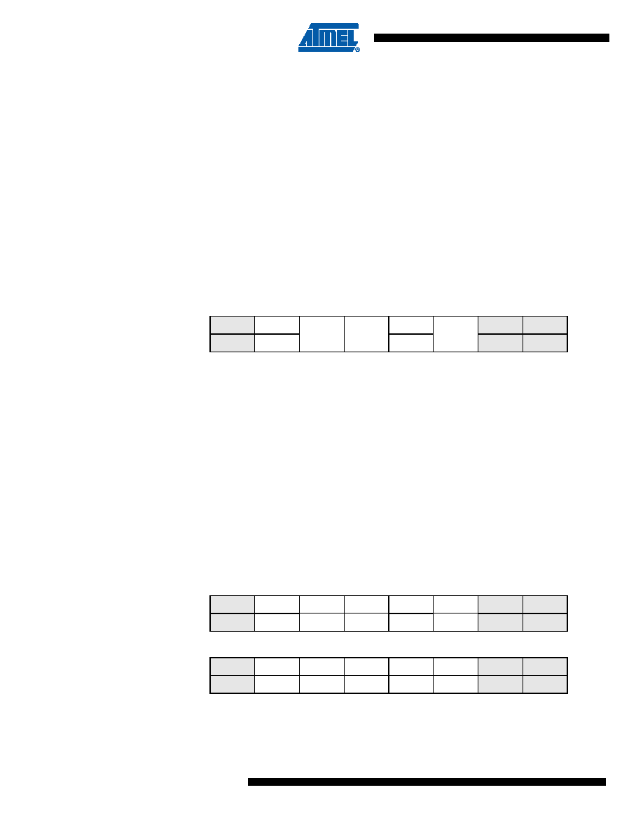
A START condition is sent by writing the following value to TWCR:
TWEN must be set to enable the Two-wire Serial Interface, STA must be written to one to trans-
mit a START condition and TWIF must be cleared. The TWI will then test the Two-wire Serial
Bus and generate a START condition as soon as the bus becomes free. After a START condi-
tion has been transmitted, the TWIF flag is set by hardware, and the status code in TWSR will be
08h (see Table 18-6). In order to enter MT mode, SLA+W must be transmitted. This is done by
writing SLA+W to TWDR. Thereafter the TWIF bit should be cleared to continue the transfer.
When SLA+W has been transmitted and an acknowledgment bit has been received, TWIF is set
again and a number of status codes in TWSR are possible. Possible status codes in Master
mode are 18h, 20h, or 38h. The appropriate action to be taken for each of these status codes is
detailed in Table 18-6.
After SLA+W has been successfully transmitted, a data packet should be transmitted. This is
done by writing the data byte to TWDR. TWDR must only be written when TWIF is high. If not,
the access will be discarded and the previous value will be transmitted. After updating TWDR,
the TWIF bit should be cleared to continue the transfer. This scheme is repeated until the last
byte has been sent and the transfer is ended by generating a STOP condition or a repeated
START condition. A STOP condition is generated by writing the following value to TWCR:
A REPEATED START condition is generated by writing the following value to TWCR:
After a repeated START condition (status 10h) the Two-wire Serial Interface can access the
same slave again, or a new slave without transmitting a STOP condition. Repeated START
enables the master to switch between slaves, Master Transmitter mode and Master Receiver
mode without losing control of the bus.
TWCR
–TWEN
STA
STO
TWIF
AA
–
Value
X
110
0
X
TWCR
–TWEN
STA
STO
TWIF
AA
–
Value
X
101
0
X
TWCR
–TWEN
STA
STO
TWIF
AA
–
Value
X
110
0
X
相关PDF资料 |
PDF描述 |
|---|---|
| VI-JTZ-IY-F4 | CONVERTER MOD DC/DC 2V 20W |
| VI-JTZ-IY-F2 | CONVERTER MOD DC/DC 2V 20W |
| ATMEGA164A-PU | IC MCU AVR 16K 20MHZ 40PDIP |
| VI-J0J-IX-B1 | CONVERTER MOD DC/DC 36V 75W |
| VI-JTZ-IY-F1 | CONVERTER MOD DC/DC 2V 20W |
相关代理商/技术参数 |
参数描述 |
|---|---|
| AT89LP4052-16PI | 功能描述:8位微控制器 -MCU Microcontroller RoHS:否 制造商:Silicon Labs 核心:8051 处理器系列:C8051F39x 数据总线宽度:8 bit 最大时钟频率:50 MHz 程序存储器大小:16 KB 数据 RAM 大小:1 KB 片上 ADC:Yes 工作电源电压:1.8 V to 3.6 V 工作温度范围:- 40 C to + 105 C 封装 / 箱体:QFN-20 安装风格:SMD/SMT |
| AT89LP4052-16PU | 功能描述:8位微控制器 -MCU Microcontroller RoHS:否 制造商:Silicon Labs 核心:8051 处理器系列:C8051F39x 数据总线宽度:8 bit 最大时钟频率:50 MHz 程序存储器大小:16 KB 数据 RAM 大小:1 KB 片上 ADC:Yes 工作电源电压:1.8 V to 3.6 V 工作温度范围:- 40 C to + 105 C 封装 / 箱体:QFN-20 安装风格:SMD/SMT |
| AT89LP4052-16SI | 功能描述:8位微控制器 -MCU Microcontroller RoHS:否 制造商:Silicon Labs 核心:8051 处理器系列:C8051F39x 数据总线宽度:8 bit 最大时钟频率:50 MHz 程序存储器大小:16 KB 数据 RAM 大小:1 KB 片上 ADC:Yes 工作电源电压:1.8 V to 3.6 V 工作温度范围:- 40 C to + 105 C 封装 / 箱体:QFN-20 安装风格:SMD/SMT |
| AT89LP4052-16SU | 功能描述:IC 8051 MCU FLASH 4K 20SOIC RoHS:是 类别:集成电路 (IC) >> 嵌入式 - 微控制器, 系列:89LP 标准包装:1,500 系列:AVR® ATtiny 核心处理器:AVR 芯体尺寸:8-位 速度:16MHz 连通性:I²C,LIN,SPI,UART/USART,USI 外围设备:欠压检测/复位,POR,PWM,温度传感器,WDT 输入/输出数:16 程序存储器容量:8KB(4K x 16) 程序存储器类型:闪存 EEPROM 大小:512 x 8 RAM 容量:512 x 8 电压 - 电源 (Vcc/Vdd):2.7 V ~ 5.5 V 数据转换器:A/D 11x10b 振荡器型:内部 工作温度:-40°C ~ 125°C 封装/外壳:20-SOIC(0.295",7.50mm 宽) 包装:带卷 (TR) |
| AT89LP4052-16XI | 功能描述:8位微控制器 -MCU Microcontroller RoHS:否 制造商:Silicon Labs 核心:8051 处理器系列:C8051F39x 数据总线宽度:8 bit 最大时钟频率:50 MHz 程序存储器大小:16 KB 数据 RAM 大小:1 KB 片上 ADC:Yes 工作电源电压:1.8 V to 3.6 V 工作温度范围:- 40 C to + 105 C 封装 / 箱体:QFN-20 安装风格:SMD/SMT |
发布紧急采购,3分钟左右您将得到回复。