- 您现在的位置:买卖IC网 > PDF目录12052 > AT89LP3240-20PU (Atmel)MCU 8051 32K FLASH 20MHZ PDF资料下载
参数资料
| 型号: | AT89LP3240-20PU |
| 厂商: | Atmel |
| 文件页数: | 57/200页 |
| 文件大小: | 0K |
| 描述: | MCU 8051 32K FLASH 20MHZ |
| 标准包装: | 10 |
| 系列: | 89LP |
| 核心处理器: | 8051 |
| 芯体尺寸: | 8-位 |
| 速度: | 20MHz |
| 连通性: | I²C,SPI,UART/USART |
| 外围设备: | 欠压检测/复位,POR,PWM,WDT |
| 输入/输出数: | 38 |
| 程序存储器容量: | 32KB(32K x 8) |
| 程序存储器类型: | 闪存 |
| EEPROM 大小: | 8K x 8 |
| RAM 容量: | 4.25K x 8 |
| 电压 - 电源 (Vcc/Vdd): | 2.4 V ~ 3.6 V |
| 数据转换器: | A/D 8x10b |
| 振荡器型: | 内部 |
| 工作温度: | -40°C ~ 85°C |
| 封装/外壳: | 40-DIP(0.540",13.72mm) |
| 包装: | 管件 |
第1页第2页第3页第4页第5页第6页第7页第8页第9页第10页第11页第12页第13页第14页第15页第16页第17页第18页第19页第20页第21页第22页第23页第24页第25页第26页第27页第28页第29页第30页第31页第32页第33页第34页第35页第36页第37页第38页第39页第40页第41页第42页第43页第44页第45页第46页第47页第48页第49页第50页第51页第52页第53页第54页第55页第56页当前第57页第58页第59页第60页第61页第62页第63页第64页第65页第66页第67页第68页第69页第70页第71页第72页第73页第74页第75页第76页第77页第78页第79页第80页第81页第82页第83页第84页第85页第86页第87页第88页第89页第90页第91页第92页第93页第94页第95页第96页第97页第98页第99页第100页第101页第102页第103页第104页第105页第106页第107页第108页第109页第110页第111页第112页第113页第114页第115页第116页第117页第118页第119页第120页第121页第122页第123页第124页第125页第126页第127页第128页第129页第130页第131页第132页第133页第134页第135页第136页第137页第138页第139页第140页第141页第142页第143页第144页第145页第146页第147页第148页第149页第150页第151页第152页第153页第154页第155页第156页第157页第158页第159页第160页第161页第162页第163页第164页第165页第166页第167页第168页第169页第170页第171页第172页第173页第174页第175页第176页第177页第178页第179页第180页第181页第182页第183页第184页第185页第186页第187页第188页第189页第190页第191页第192页第193页第194页第195页第196页第197页第198页第199页第200页
15
3706C–MICRO–2/11
AT89LP3240/6440
To enable write access to the nonvolatile data memory, the MWEN bit (MEMCON.4) must be set
to one. When MWEN = 1 and DMEN = 1, MOVX @DPTR,A may be used to write to FDATA.
FDATA uses flash memory with a page-based programming model. Flash data memory differs
from traditional EEPROM data memory in the method of writing data. EEPROM generally can
update a single byte with any value. Flash memory splits programming into write and erase
operations. A Flash write can only program zeroes, i.e change ones into zeroes (). Any
ones in the write data are ignored. A Flash erase sets an entire page of data to ones so that all
bytes become FFH. Therefore after an erase, each byte in the page can be written only once
with any possible value. Bytes can not be overwritten once they are changed from the erased
state without possibility of corrupting the data. Therefore, if even a single byte needs updating;
then the contents of the page must first be saved, the entire page must be erased and the zero
bits in all bytes (old and new data combined) must be written. Avoiding unnecessary page
erases greatly improves the endurance of the memory.
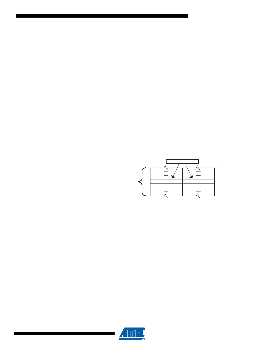
The AT89LP3240/6440 includes 64 data pages of 128 bytes each. One or more bytes in a page
may be written at one time. The AT89LP3240/6440 includes a temporary page buffer of 64
bytes, or half of a page. Because the page buffer is 64 bytes long, the maximum number of
bytes written at one time is 64. Therefore, two write cycles are required to fill the entire 128-byte
page, one for the low half page (00H–3FH) and one for the high half page (40H–7FH) as shown
in Figure 3-4.
Figure 3-4.
Page Programming Structure
The LDPG bit (MEMCON.5) allows multiple data bytes to be loaded to the temporary page buf-
fer. While LDPG = 1, MOVX @DPTR,A instructions will load data to the page buffer, but will not
start a write sequence. Note that a previously loaded byte must not be reloaded prior to the write
sequence. To write the half page into the memory, LDPG must first be cleared and then a
MOVX @DPTR,A with the final data byte is issued. The address of the final MOVX determines
which half page will be written. If a MOVX @DPTR,A instruction is issued while LDPG = 0 with-
out loading any previous bytes, only a single byte will be written. The page buffer is reset after
each write operation. Figures 3-5 and Figure 3-6 on page 16 show the difference between byte
writes and page writes.
The auto-erase bit AERS (MEMCON.6) can be set to one to perform a page erase automatically
at the beginning of any write sequence. The page erase will erase the entire page, i.e. both the
low and high half pages. However, the write operation paired with the auto-erase can only pro-
gram one of the half pages. A second write cycle without auto-erase is required to update the
other half page.
10
→
Low Half Page
00
3F
Data Memory
High Half Page
40
7F
00
3F
Page Buffer
相关PDF资料 |
PDF描述 |
|---|---|
| VI-JTZ-IY-F4 | CONVERTER MOD DC/DC 2V 20W |
| VI-JTZ-IY-F2 | CONVERTER MOD DC/DC 2V 20W |
| ATMEGA164A-PU | IC MCU AVR 16K 20MHZ 40PDIP |
| VI-J0J-IX-B1 | CONVERTER MOD DC/DC 36V 75W |
| VI-JTZ-IY-F1 | CONVERTER MOD DC/DC 2V 20W |
相关代理商/技术参数 |
参数描述 |
|---|---|
| AT89LP4052-16PI | 功能描述:8位微控制器 -MCU Microcontroller RoHS:否 制造商:Silicon Labs 核心:8051 处理器系列:C8051F39x 数据总线宽度:8 bit 最大时钟频率:50 MHz 程序存储器大小:16 KB 数据 RAM 大小:1 KB 片上 ADC:Yes 工作电源电压:1.8 V to 3.6 V 工作温度范围:- 40 C to + 105 C 封装 / 箱体:QFN-20 安装风格:SMD/SMT |
| AT89LP4052-16PU | 功能描述:8位微控制器 -MCU Microcontroller RoHS:否 制造商:Silicon Labs 核心:8051 处理器系列:C8051F39x 数据总线宽度:8 bit 最大时钟频率:50 MHz 程序存储器大小:16 KB 数据 RAM 大小:1 KB 片上 ADC:Yes 工作电源电压:1.8 V to 3.6 V 工作温度范围:- 40 C to + 105 C 封装 / 箱体:QFN-20 安装风格:SMD/SMT |
| AT89LP4052-16SI | 功能描述:8位微控制器 -MCU Microcontroller RoHS:否 制造商:Silicon Labs 核心:8051 处理器系列:C8051F39x 数据总线宽度:8 bit 最大时钟频率:50 MHz 程序存储器大小:16 KB 数据 RAM 大小:1 KB 片上 ADC:Yes 工作电源电压:1.8 V to 3.6 V 工作温度范围:- 40 C to + 105 C 封装 / 箱体:QFN-20 安装风格:SMD/SMT |
| AT89LP4052-16SU | 功能描述:IC 8051 MCU FLASH 4K 20SOIC RoHS:是 类别:集成电路 (IC) >> 嵌入式 - 微控制器, 系列:89LP 标准包装:1,500 系列:AVR® ATtiny 核心处理器:AVR 芯体尺寸:8-位 速度:16MHz 连通性:I²C,LIN,SPI,UART/USART,USI 外围设备:欠压检测/复位,POR,PWM,温度传感器,WDT 输入/输出数:16 程序存储器容量:8KB(4K x 16) 程序存储器类型:闪存 EEPROM 大小:512 x 8 RAM 容量:512 x 8 电压 - 电源 (Vcc/Vdd):2.7 V ~ 5.5 V 数据转换器:A/D 11x10b 振荡器型:内部 工作温度:-40°C ~ 125°C 封装/外壳:20-SOIC(0.295",7.50mm 宽) 包装:带卷 (TR) |
| AT89LP4052-16XI | 功能描述:8位微控制器 -MCU Microcontroller RoHS:否 制造商:Silicon Labs 核心:8051 处理器系列:C8051F39x 数据总线宽度:8 bit 最大时钟频率:50 MHz 程序存储器大小:16 KB 数据 RAM 大小:1 KB 片上 ADC:Yes 工作电源电压:1.8 V to 3.6 V 工作温度范围:- 40 C to + 105 C 封装 / 箱体:QFN-20 安装风格:SMD/SMT |
发布紧急采购,3分钟左右您将得到回复。