参数资料
| 型号: | AT90LS2343-1SI |
| 厂商: | Atmel |
| 文件页数: | 39/63页 |
| 文件大小: | 0K |
| 描述: | IC MCU 2K FLASH 1MHZ IND 8-SOIC |
| 标准包装: | 95 |
| 系列: | AVR® 90LS |
| 核心处理器: | AVR |
| 芯体尺寸: | 8-位 |
| 速度: | 1MHz |
| 连通性: | SPI |
| 外围设备: | 欠压检测/复位,POR,WDT |
| 输入/输出数: | 5 |
| 程序存储器容量: | 2KB(1K x 16) |
| 程序存储器类型: | 闪存 |
| EEPROM 大小: | 128 x 8 |
| RAM 容量: | 128 x 8 |
| 电压 - 电源 (Vcc/Vdd): | 2.7 V ~ 6 V |
| 振荡器型: | 内部 |
| 工作温度: | -40°C ~ 85°C |
| 封装/外壳: | 8-SOIC(0.209",5.30mm 宽) |
| 包装: | 管件 |
第1页第2页第3页第4页第5页第6页第7页第8页第9页第10页第11页第12页第13页第14页第15页第16页第17页第18页第19页第20页第21页第22页第23页第24页第25页第26页第27页第28页第29页第30页第31页第32页第33页第34页第35页第36页第37页第38页当前第39页第40页第41页第42页第43页第44页第45页第46页第47页第48页第49页第50页第51页第52页第53页第54页第55页第56页第57页第58页第59页第60页第61页第62页第63页
2002 Microchip Technology Inc.
Preliminary
DS41139B-page 43
PIC16C433
8.0
ANALOG-TO-DIGITAL
CONVERTER (A/D) MODULE
The Analog-to-Digital (A/D) converter module has four
analog inputs.
The A/D allows conversion of an analog input signal to
a corresponding 8-bit digital number (refer to Applica-
tion Note AN546 for use of A/D Converter). The output
of the sample and hold is the input into the converter,
which generates the result via successive approxima-
tion. The analog reference voltage is software select-
able to either the device’s positive supply voltage
(VDD), or the voltage level on the GP1/AN1/VREF pin.
The A/D converter has a unique feature of being able
to operate while the device is in SLEEP mode.
The A/D module has three registers. These registers
are:
A/D Result Register (ADRES)
A/D Control Register 0 (ADCON0)
A/D Control Register 1 (ADCON1)
The ADCON0 Register, shown in Figure 8-1, controls
the operation of the A/D module. The ADCON1 Regis-
ter, shown in Figure 8-2, configures the functions of the
port pins. The port pins can be configured as analog
inputs (GP1 can also be a voltage reference) or as
digital I/O.
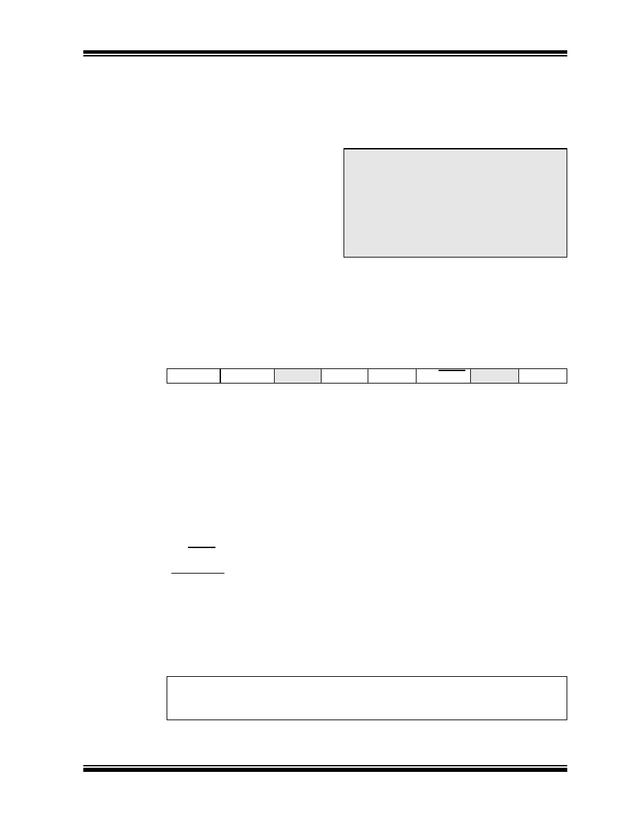
REGISTER 8-1:
ADCON0 REGISTER (ADDRESS 1Fh)
Note 1: If the port pins are configured as analog
inputs (RESET condition), reading the
port (MOVF
GPIO,W
) results in reading
'0's.
2: Changing ADCON1 Register can cause
the GPIF and INTF flags to be set in the
INTCON Register.
These interrupts
should be disabled prior to modifying
ADCON1.
R/W-0
ADCS1
ADCS0
reserved
CHS1
CHS0
GO/DONE
reserved
ADON
bit7
bit0
bit 7-6
ADCS<1:0>: A/D Conversion Clock Select bits
00
= FOSC/2
01
= FOSC/8
10
= FOSC/32
11
= FRC (clock derived from an RC oscillation)
bit 5
Reserved
bit 4-3
CHS<1:0>: Analog Channel Select bits
00
= channel 0, (GP0/AN0)
01
= channel 1, (GP1/AN1)
10
= channel 2, (GP2/AN2)
11
= channel 3, (GP4/AN3)
bit 2
GO/DONE: A/D Conversion Status bit
If ADON = 1:
1
= A/D conversion in progress (setting this bit starts the A/D conversion)
0
= A/D conversion not in progress (this bit is automatically cleared by hardware when the
A/D conversion is complete)
bit 1
Reserved
bit 0
ADON: A/D On bit
1
= A/D converter module is operating
0
= A/D converter module is shut-off and consumes no operating current
Legend:
R = Readable bit
W = Writable bit
U = Unimplemented bit, read as ‘0’
- n = Value at POR
’1’ = Bit is set
’0’ = Bit is cleared
x = Bit is unknown
相关PDF资料 |
PDF描述 |
|---|---|
| AT90PWM1-16MUR | MCU AVR 8K ISP FLASH 16MHZ 32QFN |
| AT90S1200A-4SC | MCU 1K FLASH 4MHZ LV 20-SOIC |
| AT90S2313-10PC | IC MCU 2K FLSH 10MHZ UART 20DIP |
| AT90S4433-8AC | IC MCU 4K FLSH 8MHZ A/D 32TQFP |
| AT90S8515A-8PC | IC MCU 8K FLSH 8MHZ 40DIP |
相关代理商/技术参数 |
参数描述 |
|---|---|
| AT90LS2343-4PC | 功能描述:8位微控制器 -MCU 2k bit RoHS:否 制造商:Silicon Labs 核心:8051 处理器系列:C8051F39x 数据总线宽度:8 bit 最大时钟频率:50 MHz 程序存储器大小:16 KB 数据 RAM 大小:1 KB 片上 ADC:Yes 工作电源电压:1.8 V to 3.6 V 工作温度范围:- 40 C to + 105 C 封装 / 箱体:QFN-20 安装风格:SMD/SMT |
| AT90LS2343-4PI | 功能描述:8位微控制器 -MCU 2k bit RoHS:否 制造商:Silicon Labs 核心:8051 处理器系列:C8051F39x 数据总线宽度:8 bit 最大时钟频率:50 MHz 程序存储器大小:16 KB 数据 RAM 大小:1 KB 片上 ADC:Yes 工作电源电压:1.8 V to 3.6 V 工作温度范围:- 40 C to + 105 C 封装 / 箱体:QFN-20 安装风格:SMD/SMT |
| AT90LS2343-4SC | 制造商:ATMEL 制造商全称:ATMEL Corporation 功能描述:8-Bit Microcontroller with 2K Bytes of In-System Programmable Flash |
| AT90LS2343-4SI | 功能描述:8位微控制器 -MCU 2k bit RoHS:否 制造商:Silicon Labs 核心:8051 处理器系列:C8051F39x 数据总线宽度:8 bit 最大时钟频率:50 MHz 程序存储器大小:16 KB 数据 RAM 大小:1 KB 片上 ADC:Yes 工作电源电压:1.8 V to 3.6 V 工作温度范围:- 40 C to + 105 C 封装 / 箱体:QFN-20 安装风格:SMD/SMT |
| AT90LS2343-4SI SL383 | 制造商:Atmel Corporation 功能描述:4MHZSOICIND TEMP3.0V |
发布紧急采购,3分钟左右您将得到回复。