参数资料
| 型号: | ATMEGA324PA-MCH |
| 厂商: | Atmel |
| 文件页数: | 127/160页 |
| 文件大小: | 0K |
| 描述: | MCU AVR 32KB FLASH 44-VQFN |
| 产品培训模块: | MCU Product Line Introduction megaAVR Introduction |
| 标准包装: | 490 |
| 系列: | AVR® ATmega |
| 核心处理器: | AVR |
| 芯体尺寸: | 8-位 |
| 速度: | 20MHz |
| 连通性: | I²C,SPI,UART/USART |
| 外围设备: | 欠压检测/复位,POR,PWM,WDT |
| 输入/输出数: | 32 |
| 程序存储器容量: | 32KB(16K x 16) |
| 程序存储器类型: | 闪存 |
| EEPROM 大小: | 1K x 8 |
| RAM 容量: | 2K x 8 |
| 电压 - 电源 (Vcc/Vdd): | 1.8 V ~ 5.5 V |
| 数据转换器: | A/D 8x10b |
| 振荡器型: | 内部 |
| 工作温度: | -40°C ~ 85°C |
| 封装/外壳: | 44-VQFN 裸露焊盘 |
| 包装: | 托盘 |
| 配用: | ATSTK600-ND - DEV KIT FOR AVR/AVR32 |
第1页第2页第3页第4页第5页第6页第7页第8页第9页第10页第11页第12页第13页第14页第15页第16页第17页第18页第19页第20页第21页第22页第23页第24页第25页第26页第27页第28页第29页第30页第31页第32页第33页第34页第35页第36页第37页第38页第39页第40页第41页第42页第43页第44页第45页第46页第47页第48页第49页第50页第51页第52页第53页第54页第55页第56页第57页第58页第59页第60页第61页第62页第63页第64页第65页第66页第67页第68页第69页第70页第71页第72页第73页第74页第75页第76页第77页第78页第79页第80页第81页第82页第83页第84页第85页第86页第87页第88页第89页第90页第91页第92页第93页第94页第95页第96页第97页第98页第99页第100页第101页第102页第103页第104页第105页第106页第107页第108页第109页第110页第111页第112页第113页第114页第115页第116页第117页第118页第119页第120页第121页第122页第123页第124页第125页第126页当前第127页第128页第129页第130页第131页第132页第133页第134页第135页第136页第137页第138页第139页第140页第141页第142页第143页第144页第145页第146页第147页第148页第149页第150页第151页第152页第153页第154页第155页第156页第157页第158页第159页第160页
69
8272E–AVR–04/2013
ATmega164A/PA/324A/PA/644A/PA/1284/P
is executed. Alternatively, the flag can be cleared by writing a logical one to it. These flags are
always cleared when INT2:0 are configured as level interrupt. Note that when entering sleep
mode with the INT2:0 interrupts disabled, the input buffers on these pins will be disabled. This
may cause a logic change in internal signals which will set the INTF2:0 flags. See ”Digital Input
Enable and Sleep Modes” on page 76 for more information.
13.2.4
PCICR – Pin Change Interrupt Control Register
Bit 3 – PCIE3: Pin Change Interrupt Enable 3
When the PCIE3 bit is set (one) and the I-bit in the Status Register (SREG) is set (one), pin
change interrupt 3 is enabled. Any change on any enabled PCINT31:24 pin will cause an inter-
rupt. The corresponding interrupt of Pin Change Interrupt Request is executed from the PCI3
Interrupt Vector. PCINT31:24 pins are enabled individually by the PCMSK3 Register.
Bit 2 – PCIE2: Pin Change Interrupt Enable 2
When the PCIE2 bit is set (one) and the I-bit in the Status Register (SREG) is set (one), pin
change interrupt 2 is enabled. Any change on any enabled PCINT23:16 pin will cause an inter-
rupt. The corresponding interrupt of Pin Change Interrupt Request is executed from the PCI2
Interrupt Vector. PCINT23:16 pins are enabled individually by the PCMSK2 Register.
Bit 1 – PCIE1: Pin Change Interrupt Enable 1
When the PCIE1 bit is set (one) and the I-bit in the Status Register (SREG) is set (one), pin
change interrupt 1 is enabled. Any change on any enabled PCINT15:8 pin will cause an inter-
rupt. The corresponding interrupt of Pin Change Interrupt Request is executed from the PCI1
Interrupt Vector. PCINT15:8 pins are enabled individually by the PCMSK1 Register.
Bit 0 – PCIE0: Pin Change Interrupt Enable 0
When the PCIE0 bit is set (one) and the I-bit in the Status Register (SREG) is set (one), pin
change interrupt 0 is enabled. Any change on any enabled PCINT7:.0 pin will cause an interrupt.
The corresponding interrupt of Pin Change Interrupt Request is executed from the PCI0 Interrupt
Vector. PCINT7:0 pins are enabled individually by the PCMSK0 Register.
13.2.5
PCIFR – Pin Change Interrupt Flag Register
Bit 3– PCIF3: Pin Change Interrupt Flag 3
When a logic change on any PCINT31:24 pin triggers an interrupt request, PCIF3 becomes set
(one). If the I-bit in SREG and the PCIE3 bit in PCICR are set (one), the MCU will jump to the
corresponding Interrupt Vector. The flag is cleared when the interrupt routine is executed. Alter-
natively, the flag can be cleared by writing a logical one to it.
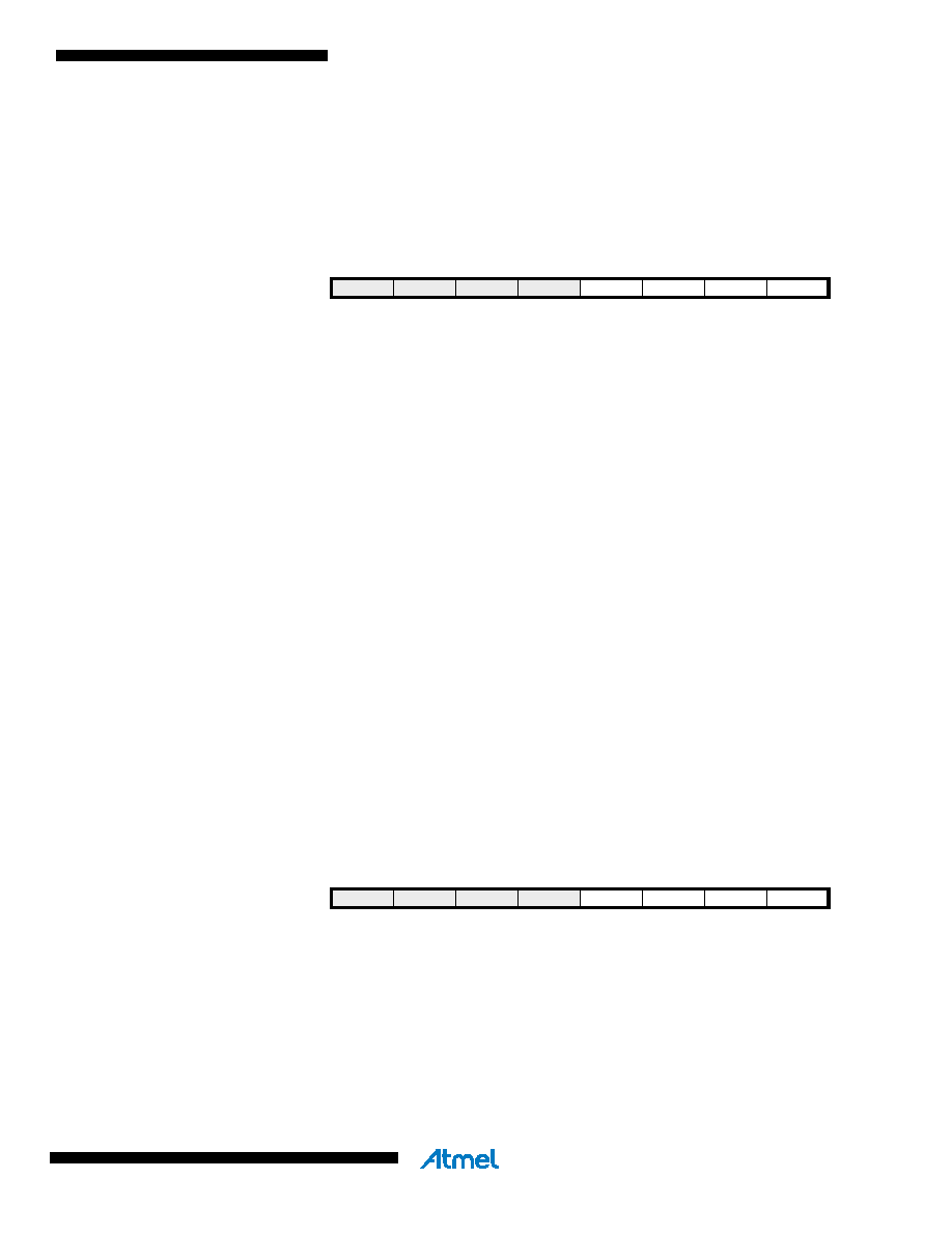
Bit
7
6543
210
–
PCIE3
PCIE2
PCIE1
PCIE0
PCICR
Read/Write
RRRR
R/W
Initial Value
0
0000
000
Bit
7
6543
210
–
PCIF3
PCIF2
PCIF1
PCIF0
PCIFR
Read/Write
RRRR
R/W
Initial Value
0
0000
000
相关PDF资料 |
PDF描述 |
|---|---|
| ATMEGA324PA-PU | MCU AVR 32KB FLASH 40PDIP |
| ATSAM3N4AA-MU | MCU FLASH 48-QFN |
| ATMEGA48P-20AU | MCU AVR 4K ISP FLSH 20MHZ 32TQFP |
| ATTINY84-20PU | IC MCU AVR 8K FLASH 20MHZ 14-DIP |
| ATTINY84V-10PU | IC MCU AVR 8K FLASH 10MHZ 14-DIP |
相关代理商/技术参数 |
参数描述 |
|---|---|
| ATMEGA324PA-MCHR | 功能描述:8位微控制器 -MCU AVR 32KB FLSH 1KB EE 2KB SRAM-20MHz IND RoHS:否 制造商:Silicon Labs 核心:8051 处理器系列:C8051F39x 数据总线宽度:8 bit 最大时钟频率:50 MHz 程序存储器大小:16 KB 数据 RAM 大小:1 KB 片上 ADC:Yes 工作电源电压:1.8 V to 3.6 V 工作温度范围:- 40 C to + 105 C 封装 / 箱体:QFN-20 安装风格:SMD/SMT |
| ATMEGA324PA-MN | 功能描述:8位微控制器 -MCU AVR 32KB FLSH 1KB EE 2KB SRAM-20MHz 105C RoHS:否 制造商:Silicon Labs 核心:8051 处理器系列:C8051F39x 数据总线宽度:8 bit 最大时钟频率:50 MHz 程序存储器大小:16 KB 数据 RAM 大小:1 KB 片上 ADC:Yes 工作电源电压:1.8 V to 3.6 V 工作温度范围:- 40 C to + 105 C 封装 / 箱体:QFN-20 安装风格:SMD/SMT |
| ATMEGA324PA-MNR | 功能描述:20 MHZ, QFP, 105C 制造商:microchip technology 系列:AVR? ATmega 包装:剪切带(CT) 零件状态:在售 核心处理器:AVR 核心尺寸:8-位 速度:20MHz 连接性:I2C,SPI,UART/USART 外设:欠压检测/复位,POR,PWM,WDT I/O 数:32 程序存储容量:32KB(16K x 16) 程序存储器类型:闪存 EEPROM 容量:1K x 8 RAM 容量:2K x 8 电压 - 电源(Vcc/Vdd):1.8 V ~ 5.5 V 数据转换器:A/D 8x10b 振荡器类型:内部 工作温度:-40°C ~ 105°C(TA) 封装/外壳:44-VFQFN 裸露焊盘 供应商器件封装:44-VQFN(7x7) 标准包装:1 |
| ATMEGA324PA-MU | 功能描述:8位微控制器 -MCU AVR 32KB 1KB EE 20MHz 2KB SRAM 5V RoHS:否 制造商:Silicon Labs 核心:8051 处理器系列:C8051F39x 数据总线宽度:8 bit 最大时钟频率:50 MHz 程序存储器大小:16 KB 数据 RAM 大小:1 KB 片上 ADC:Yes 工作电源电压:1.8 V to 3.6 V 工作温度范围:- 40 C to + 105 C 封装 / 箱体:QFN-20 安装风格:SMD/SMT |
| ATMEGA324PA-MUR | 功能描述:8位微控制器 -MCU AVR 32KB FLSH 1KB EE 2KB SRAM-20MHz IND RoHS:否 制造商:Silicon Labs 核心:8051 处理器系列:C8051F39x 数据总线宽度:8 bit 最大时钟频率:50 MHz 程序存储器大小:16 KB 数据 RAM 大小:1 KB 片上 ADC:Yes 工作电源电压:1.8 V to 3.6 V 工作温度范围:- 40 C to + 105 C 封装 / 箱体:QFN-20 安装风格:SMD/SMT |
发布紧急采购,3分钟左右您将得到回复。