参数资料
| 型号: | BR34L02FVT-WE2 |
| 厂商: | Rohm Semiconductor |
| 文件页数: | 12/18页 |
| 文件大小: | 0K |
| 描述: | IC EEPROM I2C SPD 2KB 8-TSSOP |
| 标准包装: | 1 |
| 格式 - 存储器: | EEPROMs - 串行 |
| 存储器类型: | EEPROM |
| 存储容量: | 2K (256 x 8) |
| 速度: | 400kHz |
| 接口: | I²C,2 线串口 |
| 电源电压: | 1.7 V ~ 5.5 V |
| 工作温度: | -40°C ~ 85°C |
| 封装/外壳: | 8-TSSOP(0.173",4.40mm 宽) |
| 供应商设备封装: | 8-TSSOP-B |
| 包装: | 标准包装 |
| 其它名称: | BR34L02FVT-WE2DKR |
�� �
�
�BR34L02FV-W�
�Technical� Note�
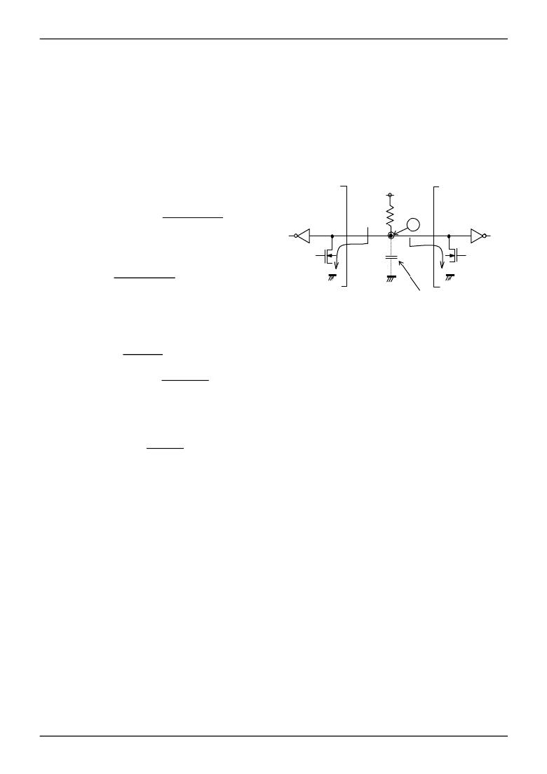
�●� I/O� Circuit�
�○� SDA� Pin� Pull-up� Resistor�
�A� pull-up� resistor� is� required� because� SDA� is� an� NMOS� open� drain.� Determine� the� resistor� value� of� (R� PU� )� by� considering�
�the� VIL� and� IL,� and� VOL-IOL� characteristics.� If� a� large� R� PU� is� chosen,� the� clock� frequency� needs� to� be� slow.� A� smaller�
�R� PU� will� result� in� a� larger� operating� current.�
�○� Maximum� R� PU�
�The� maximum� of� R� PU� can� be� determined� by� the� following� factors.�
�①� The� SDA� rise� time� determined� by� R� PU� and� the� capacitance� of� the� BUS� line(CBUS)� must� be� less� than� tR.�
�In� addition,� all� other� timings� must� be� kept� within� the� AC� specifications.�
�②� When� the� SDA� BUS� is� High,� the� voltage� A� at� the� SDA� BUS� is� determined� from� the� total� input� leakage(IL)� of� all� devices�
�connected� to� the� BUS.� R� PU� must� be� higher� than� the� input� High� level� of� the� microcontroller� and� the� device,� including� a�
�noise� margin� 0.2V� CC� .�
�V� CC� -I� L� R� PU� -0.2� V� CC� ≧� VIH�
�Microcontroller�
�BR34L02FV-W�
�∴�
�R� PU�
�≦�
�0.8V� CC� -V� IH�
�IL�
�R� PU�
�A�
�SDA� PIN�
�Examples:� When� V� CC� =3V,� IL=10μA,� VIH=0.7� V� CC�
�According� to� ②�
�IL�
�IL�
�R� PU�
�≦�
�0.8×3-0.7×3�
�10×10� -6�
�≦� 300� [� k� ?� ]�
�○� Minimum� R� PU�
�The� minimum� value� of� R� PU� is� determined� by� following� factors.�
�①� Meets� the� condition� that� V� OLMAX� =0.4V,� I� OLMAX� =3mA� when� the� output� is� Low.�
�THE� CAPACITANCE�
�OF� BUS� LINE� (CBUS)�
�Fig.43� I/O� Circuit�
�V� CC� -V� OL�
�R� PU�
�≦� I� OL�
�∴�
�R� PU� ≧�
�V� CC� -V� OL�
�I� OL�
�②� V� OLMAX� =0.4V� must� be� lower� than� the� input� Low� level� of� the� microcontroller� and� the� EEPROM�
�including� the� recommended� noise� margin� of� 0.1V� CC� .�
�V� OLMAX� ≦� VIL-0.1� V� CC�
�R� PU� ≧�
�3-0.4�
�3×10� -3�
�≧� 867� [� ?� ]�
�and�
�V� OL� =0.4� [� V� ]�
�V� IL� =0.3� � 3�
�=0.9� [� V� ]�
�so� that� condition� ②� is� met�
�○� SCL� Pin� Pull-up� Resistor�
�When� SCL� is� controlled� by� the� CMOS� output� the� pull-up� resistor� at� SCL� is� not� required.�
�However,� should� SCL� be� set� to� Hi-Z,� connection� of� a� pull-up� resistor� between� SCL� and� V� CC� is� recommended.�
�Several� k� ?� are� recommended� for� the� pull-up� resistor� in� order� to� drive� the� output� port� of� the� microcontroller.�
�●� A0,� A1,� A2,� WP� Pin� connections�
�○� Device� Address� Pin� (A0,� A1,� A2)� connections�
�The� status� of� the� device� address� pins� is� compared� with� the� device� address� sent� by� the� Master.� One� of� the� devices� that� is�
�connected� to� the� identical� BUS� is� selected.� Pull� up� or� down� these� pins� or� connect� them� to� V� CC� or� GND.� Pins� that� are� not�
�used� as� device� address� (N.C.Pins)� may� be� High,� Low,� or� Hi-Z.�
�WP� Pin� connection�
�The� WP� input� allows� or� prohibits� write� operations.� When� WP� is� High,� only� Read� is� available� and� Write� to� all� address� is�
�prohibited.� Both� Read� and� Write� are� available� when� WP� is� Low.�
�In� the� event� that� the� device� is� used� as� a� ROM,� it� is� recommended� that� the� WP� input� be� pulled� up� or� connected� to� V� CC� .�
�When� both� READ� and� WRITE� are� operated,� the� WP� input� must� be� pulled� down� or� connected� to� GND� or� controlled.�
�www.rohm.com�
�?� 2009� ROHM� Co.,� Ltd.� All� rights� reserved.�
�12/17�
�2009.04� -� Rev.A�
�相关PDF资料 |
PDF描述 |
|---|---|
| AGL125V5-FG144 | IC FPGA 1KB FLASH 125K 144FBGA |
| A3P060-CS121I | IC FPGA 1KB FLASH 60K 121-CSP |
| BR24T64F-WE2 | IC EEPROM I2C 64K 400KHZ 8-SOP |
| A3P060-CSG121I | IC FPGA 1KB FLASH 60K 121-CSP |
| AGL030V2-CSG81I | IC FPGA 1KB FLASH 30K 81-CSP |
相关代理商/技术参数 |
参数描述 |
|---|---|
| BR34L02FVT-WSE2 | 制造商:ROHM Semiconductor 功能描述:IC EEPROM |
| BR34L02FV-W | 制造商:ROHM 制造商全称:Rohm 功能描述:DDR1/DDR2 For memory module) SPD Memory |
| BR34L02FV-W_09 | 制造商:ROHM 制造商全称:Rohm 功能描述:DDR1/DDR2 For memory module) SPD Memory |
| BR34L02FV-WE2 | 功能描述:电可擦除可编程只读存储器 SRL 256X8 BIT RoHS:否 制造商:Atmel 存储容量:2 Kbit 组织:256 B x 8 数据保留:100 yr 最大时钟频率:1000 KHz 最大工作电流:6 uA 工作电源电压:1.7 V to 5.5 V 最大工作温度:+ 85 C 安装风格:SMD/SMT 封装 / 箱体:SOIC-8 |
| BR34L02-W | 制造商:ROHM 制造商全称:Rohm 功能描述:2Kbit Serial I2C BUS EEPROM For SPD DRAM Memory Module |
发布紧急采购,3分钟左右您将得到回复。