- 您现在的位置:买卖IC网 > PDF目录256019 > BU-61840B3-100L (DATA DEVICE CORP) 2 CHANNEL(S), 1M bps, MIL-STD-1553 CONTROLLER, PBGA128 PDF资料下载
参数资料
| 型号: | BU-61840B3-100L |
| 厂商: | DATA DEVICE CORP |
| 元件分类: | 微控制器/微处理器 |
| 英文描述: | 2 CHANNEL(S), 1M bps, MIL-STD-1553 CONTROLLER, PBGA128 |
| 封装: | 0.815 X 0.815 INCH, 0.140 INCH HEIGHT, BGA-128 |
| 文件页数: | 30/60页 |
| 文件大小: | 763K |
| 代理商: | BU-61840B3-100L |
第1页第2页第3页第4页第5页第6页第7页第8页第9页第10页第11页第12页第13页第14页第15页第16页第17页第18页第19页第20页第21页第22页第23页第24页第25页第26页第27页第28页第29页当前第30页第31页第32页第33页第34页第35页第36页第37页第38页第39页第40页第41页第42页第43页第44页第45页第46页第47页第48页第49页第50页第51页第52页第53页第54页第55页第56页第57页第58页第59页第60页
36
Data Device Corporation
www.ddc-web.com
BU-6174X/6184X/6186X
D-03/02-250
CLOCK IN
VALID
t7
t3
t8
t11
t13
t15
VALID
t10
t4
t9
t12
t19
;
;;
VALID
t16
t17
SELECT
(Note 2,7)
(Note 2)
(Note 3,4,7)
(Note 4,5)
STRBD
MEM/REG
RD/WR
IOEN
(Note 2,6)
(Note 6)
(Note 7,8,9)
READYD
A15-A0
D15-D0
;
;;
;;;
;;
t5
t1
t2
t6
t14
t18
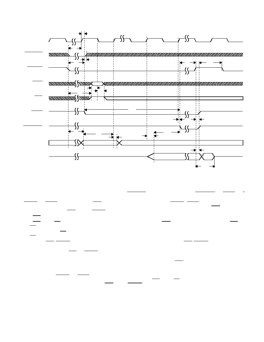
FIGURE 13. CPU READING RAM / REGISTER (16-BIT BUFFERED, NONZERO WAIT)
NOTES:
1.
For the 16-bit buffered nonzero wait configuration, TRANSPARENT/BUFFERED must be connected to logic "0". ZERO_WAIT and DTREQ / 16/8
must be connected to logic "1". The inputs TRIGGER_SEL and MSB/LSB may be connected to either +5V or ground.
2.
SELECT and STRBD may be tied together. IOEN goes low on the first rising CLK edge when SELECT STRBD is sampled low (satisfying t1)
and the Enhanced Mini-ACE's protocol/memory management logic is not accessing the internal RAM. When this occurs, IOEN goes low, start-
ing the transfer cycle. After IOEN goes low, SELECT may be released high.
3.
MEM/REG must be presented high for memory access, low for register access.
4.
MEM/REG and RD/WR are buffered transparently until the first falling edge of CLK after IOEN goes low. After this CLK edge, MEM/REG and
RD/WR become latched internally.
5.
The logic sense for RD/WR in the diagram assumes that POLARITY_SEL is connected to logic "1." If POLARITY_SEL is connected to logic "0,"
RD/WR must be asserted low to read.
6.
The timing for IOEN, READYD and D15-D0 assumes a 50 pf load. For loading above 50 pf, the validity of IOEN, READYD, and D15-D0 is delayed
by an additional 0.14 ns/pf typ, 0.28 ns/pf max.
7.
The timing for A15-A0, MEM/REG and SELECT assumes that ADDR-LAT is connected to logic "1." Refer to Address Latch timing for additional
details.
8.
The address bus A15-A0 is internally buffered transparently until the first rising edge of CLK after IOEN goes low. After this CLK edge, A15-A0
become latched internally.
9.
Setup time given for use in worst case timing calculations. None of the Enhanced Mini-ACE input signals are required to be synchronized to the
system clock. When SELECT and STRBD do not meet the setup time of t1, but occur during the setup window of an internal flip-flop, an addi-
tional clock cycle will be inserted between the falling clock edge that latches MEM/REG and RD/WR and the rising clock edge that latches the
Address (A15-A0). When this occurs, the delay from IOEN falling to READYD falling (t11) increases by one clock cycle and the address hold time
(t10) must be increased be one clock cycle.
相关PDF资料 |
PDF描述 |
|---|---|
| BU-61840B3-300Y | 2 CHANNEL(S), 1M bps, MIL-STD-1553 CONTROLLER, PBGA128 |
| BU-61860B3-102 | 2 CHANNEL(S), 1M bps, MIL-STD-1553 CONTROLLER, PBGA128 |
| BU-61860B3-402W | 2 CHANNEL(S), 1M bps, MIL-STD-1553 CONTROLLER, PBGA128 |
| BU-61860B4-100Z | 2 CHANNEL(S), 1M bps, MIL-STD-1553 CONTROLLER, PBGA128 |
| BU-61860B4-200S | 2 CHANNEL(S), 1M bps, MIL-STD-1553 CONTROLLER, PBGA128 |
相关代理商/技术参数 |
参数描述 |
|---|---|
| BU-61840B3NEW | 制造商:未知厂家 制造商全称:未知厂家 功能描述:MIL-STD-1553 Components |μ-ACE (Micro-ACE?) |
| BU-61843 | 制造商:未知厂家 制造商全称:未知厂家 功能描述:MIL-STD-1553 Components |Enhanced Mini-ACE? |
| BU-61843F3-100 | 制造商:未知厂家 制造商全称:未知厂家 功能描述:Telecommunication IC |
| BU-61843F3-110 | 制造商:未知厂家 制造商全称:未知厂家 功能描述:Telecommunication IC |
| BU-61843F4-100 | 制造商:未知厂家 制造商全称:未知厂家 功能描述:Telecommunication IC |
发布紧急采购,3分钟左右您将得到回复。