- 您现在的位置:买卖IC网 > PDF目录256019 > BU-61840B3-100L (DATA DEVICE CORP) 2 CHANNEL(S), 1M bps, MIL-STD-1553 CONTROLLER, PBGA128 PDF资料下载
参数资料
| 型号: | BU-61840B3-100L |
| 厂商: | DATA DEVICE CORP |
| 元件分类: | 微控制器/微处理器 |
| 英文描述: | 2 CHANNEL(S), 1M bps, MIL-STD-1553 CONTROLLER, PBGA128 |
| 封装: | 0.815 X 0.815 INCH, 0.140 INCH HEIGHT, BGA-128 |
| 文件页数: | 43/60页 |
| 文件大小: | 763K |
| 代理商: | BU-61840B3-100L |
第1页第2页第3页第4页第5页第6页第7页第8页第9页第10页第11页第12页第13页第14页第15页第16页第17页第18页第19页第20页第21页第22页第23页第24页第25页第26页第27页第28页第29页第30页第31页第32页第33页第34页第35页第36页第37页第38页第39页第40页第41页第42页当前第43页第44页第45页第46页第47页第48页第49页第50页第51页第52页第53页第54页第55页第56页第57页第58页第59页第60页
48
Data Device Corporation
www.ddc-web.com
BU-6174X/6184X/6186X
D-03/02-250
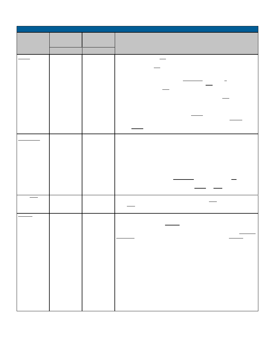
POL_SEL (I) /
DTACK (O)
29
Data Transfer Acknowledge or Polarity Select. In 16-bit buffered mode, if POL_SEL is
connected to logic "1", RD/WR should be asserted high (logic "1") for a read operation
and low (logic "0") for a write operation. In 16-bit buffered mode, if POL_SEL is con-
nected to logic "0", RD/WR should be asserted low (logic "0") for a read operation and
high (logic "1") for a write operation.
In 8-bit buffered mode (TRANSPARENT/ BUFFERED = “0" and 16/8 = "0"), POL_SEL
input signal used to control the logic sense of the MSB/LSB signal. If POL_SEL is
connected to logic “0", MSB/LSB should be asserted low (logic "0") to indicate the
transfer of the least significant byte and high (logic "1") to indicate the transfer of the
most significant byte. If POL_SEL is connected to logic “1", MSB/LSB should be
asserted high (logic "1") to indicate the transfer of the least significant byte and low
(logic "0") to indicate the transfer of the most significant byte.
In transparent mode, active low output signal (DTACK) used to indicate acceptance of
the processor/RAM interface bus in response to a data transfer grant (DTGRT). The
Enhanced Mini-ACE's RAM transfers over A15-A0 and D15-D0 will be framed by the
time that DTACK is asserted low.
U7
TRIG_SEL (I) /
MEMENA_IN (I)
28
Memory Enable or Trigger Select input. In 8-bit buffered mode, input signal (TRIG-SEL)
used to select the order in which byte pairs are transferred to or from the Enhanced
MINI-ACE by the host processor. In the 8-bit buffered mode, TRIG_SEL should be
asserted high (logic 1) if the byte order for both read operations and write operations is
MSB followed by LSB. TRIG_SEL should be asserted low (logic 0) if the byte order for
both read operations and write operations is LSB followed by MSB.
This signal has no operation in the 16-bit buffered mode (it does not need to be con-
nected).
In transparent mode, active low input MEMENA_IN, used as a Chip Select (CS) input to the
Enhanced Mini-ACE's internal shared RAM. If only internal RAM is used, should be connect-
ed directly to the output of a gate that is OR'ing the DTACK and IOEN output signals.
V6
MEM / REG(I)
1
Memory/Register. Generally connected to either a CPU address line or address
decoder output. Selects between memory access (MEM/REG = "1") or register access
(MEM/REG = "0").
B13
SSFLAG (I) /
EXT_TRIG(I)
32
Subsystem Flag (RT) or External Trigger (BC/Word Monitor) input. In RT mode, if this
input is asserted low, the Subsystem Flag bit will be set in the ENHANCED MINI-
ACE's RT Status Word. If the SSFLAG input is logic "0" while bit 8 of Configuration
Register #1 has been programmed to logic "1" (cleared), the Subsystem Flag RT
Status Word bit will become logic "1," but bit 8 of Configuration Register #1, SUBSYS-
TEM FLAG, will return logic "1" when read. That is, the sense on the SSFLAG input
has no effect on the SUBSYSTEM FLAG register bit.
In the non-enhanced BC mode, this signal operates as an External Trigger input. In
BC mode, if the external BC Start option is enabled (bit 7 of Configuration Register
#1), a low to high transition on this input will issue a BC Start command, starting exe-
cution of the current BC frame.
In the enhanced BC mode, during the execution of a Wait for External Trigger (WTG)
instruction, the Enhanced Mini-ACE BC will wait for a low-to-high transition on
EXT_TRIG before proceeding to the next instruction.
In the Word Monitor mode, if the external trigger is enabled (bit 7 of Configuration
Register #1), a low to high transition on this input will initiate a monitor start.
This input has no effect in Message Monitor mode.
T2
TABLE 51. PROCESSOR INTERFACE CONTROL (CONT.)
SIGNAL NAME
DESCRIPTION
BU-6186XFX/GX
BU-6184XFX/GX
BU-6174XFX/GX
BALL
PIN
BU-61860BX
BU-61840BX
BU-61740BX
相关PDF资料 |
PDF描述 |
|---|---|
| BU-61840B3-300Y | 2 CHANNEL(S), 1M bps, MIL-STD-1553 CONTROLLER, PBGA128 |
| BU-61860B3-102 | 2 CHANNEL(S), 1M bps, MIL-STD-1553 CONTROLLER, PBGA128 |
| BU-61860B3-402W | 2 CHANNEL(S), 1M bps, MIL-STD-1553 CONTROLLER, PBGA128 |
| BU-61860B4-100Z | 2 CHANNEL(S), 1M bps, MIL-STD-1553 CONTROLLER, PBGA128 |
| BU-61860B4-200S | 2 CHANNEL(S), 1M bps, MIL-STD-1553 CONTROLLER, PBGA128 |
相关代理商/技术参数 |
参数描述 |
|---|---|
| BU-61840B3NEW | 制造商:未知厂家 制造商全称:未知厂家 功能描述:MIL-STD-1553 Components |μ-ACE (Micro-ACE?) |
| BU-61843 | 制造商:未知厂家 制造商全称:未知厂家 功能描述:MIL-STD-1553 Components |Enhanced Mini-ACE? |
| BU-61843F3-100 | 制造商:未知厂家 制造商全称:未知厂家 功能描述:Telecommunication IC |
| BU-61843F3-110 | 制造商:未知厂家 制造商全称:未知厂家 功能描述:Telecommunication IC |
| BU-61843F4-100 | 制造商:未知厂家 制造商全称:未知厂家 功能描述:Telecommunication IC |
发布紧急采购,3分钟左右您将得到回复。