- 您现在的位置:买卖IC网 > PDF目录298892 > BX80547RE2533C (INTEL CORP) 32-BIT, 2530 MHz, MICROPROCESSOR, PBGA775 PDF资料下载
参数资料
| 型号: | BX80547RE2533C |
| 厂商: | INTEL CORP |
| 元件分类: | 微控制器/微处理器 |
| 英文描述: | 32-BIT, 2530 MHz, MICROPROCESSOR, PBGA775 |
| 封装: | FLIP CHIP, LGA-775 |
| 文件页数: | 53/94页 |
| 文件大小: | 2796K |
| 代理商: | BX80547RE2533C |
第1页第2页第3页第4页第5页第6页第7页第8页第9页第10页第11页第12页第13页第14页第15页第16页第17页第18页第19页第20页第21页第22页第23页第24页第25页第26页第27页第28页第29页第30页第31页第32页第33页第34页第35页第36页第37页第38页第39页第40页第41页第42页第43页第44页第45页第46页第47页第48页第49页第50页第51页第52页当前第53页第54页第55页第56页第57页第58页第59页第60页第61页第62页第63页第64页第65页第66页第67页第68页第69页第70页第71页第72页第73页第74页第75页第76页第77页第78页第79页第80页第81页第82页第83页第84页第85页第86页第87页第88页第89页第90页第91页第92页第93页第94页
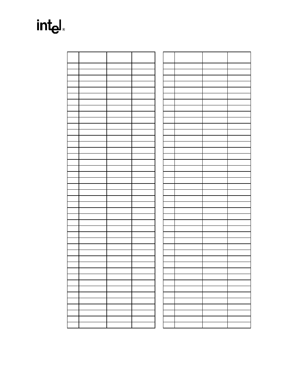
Land Listing and Signal Descriptions
Datasheet
57
R8
VCC
Power/Other
—
R23
VSS
Power/Other
—
R24
VSS
Power/Other
—
R25
VSS
Power/Other
—
R26
VSS
Power/Other
—
R27
VSS
Power/Other
—
R28
VSS
Power/Other
—
R29
VSS
Power/Other
—
R30
VSS
Power/Other
—
T1
COMP1
Power/Other
Input
T2
COMP5
Power/Other
Input
T3
VSS
Power/Other
—
T4
A11#
Source Synch
Input/Output
T5
A9#
Source Synch
Input/Output
T6
VSS
Power/Other
—
T7
VSS
Power/Other
—
T8
VCC
Power/Other
—
T23
VCC
Power/Other
—
T24
VCC
Power/Other
—
T25
VCC
Power/Other
—
T26
VCC
Power/Other
—
T27
VCC
Power/Other
—
T28
VCC
Power/Other
—
T29
VCC
Power/Other
—
T30
VCC
Power/Other
—
U1
VSS
Power/Other
—
U2
AP0#
Common Clock
Input/Output
U3
AP1#
Common Clock
Input/Output
U4
A13#
Source Synch
Input/Output
U5
A12#
Source Synch
Input/Output
U6
A10#
Source Synch
Input/Output
U7
VSS
Power/Other
—
U8
VCC
Power/Other
—
U23
VCC
Power/Other
—
U24
VCC
Power/Other
—
U25
VCC
Power/Other
—
U26
VCC
Power/Other
—
U27
VCC
Power/Other
—
U28
VCC
Power/Other
—
U29
VCC
Power/Other
—
U30
VCC
Power/Other
—
V1
MS_ID1
Power/Other
Output
V2
LL_ID0
Power/Other
Output
V3
VSS
Power/Other
—
Table 4-2. Numerical Land Assignments
Land
#
Land Name
Signal Buffer
Type
Direction
V4
A15#
Source Synch
Input/Output
V5
A14#
Source Synch
Input/Output
V6
VSS
Power/Other
—
V7
VSS
Power/Other
—
V8
VCC
Power/Other
—
V23
VSS
Power/Other
—
V24
VSS
Power/Other
—
V25
VSS
Power/Other
—
V26
VSS
Power/Other
—
V27
VSS
Power/Other
—
V28
VSS
Power/Other
—
V29
VSS
Power/Other
—
V30
VSS
Power/Other
—
W1
MS_ID0
Power/Other
Output
W2
TESTHI12
Power/Other
Input
W3
TESTHI1
Power/Other
Input
W4
VSS
Power/Other
—
W5
A16#
Source Synch
Input/Output
W6
A18#
Source Synch
Input/Output
W7
VSS
Power/Other
—
W8
VCC
Power/Other
—
W23
VCC
Power/Other
—
W24
VCC
Power/Other
—
W25
VCC
Power/Other
—
W26
VCC
Power/Other
—
W27
VCC
Power/Other
—
W28
VCC
Power/Other
—
W29
VCC
Power/Other
—
W30
VCC
Power/Other
—
Y1
BOOTSELECT
Power/Other
Input
Y2
VSS
Power/Other
—
Y3
RESERVED
—
Y4
A20#
Source Synch
Input/Output
Y5
VSS
Power/Other
—
Y6
A19#
Source Synch
Input/Output
Y7
VSS
Power/Other
—
Y8
VCC
Power/Other
—
Y23
VCC
Power/Other
—
Y24
VCC
Power/Other
—
Y25
VCC
Power/Other
—
Y26
VCC
Power/Other
—
Y27
VCC
Power/Other
—
Y28
VCC
Power/Other
—
Y29
VCC
Power/Other
—
Table 4-2. Numerical Land Assignments
Land
#
Land Name
Signal Buffer
Type
Direction
相关PDF资料 |
PDF描述 |
|---|---|
| BX80547RE2667C | 32-BIT, 2600 MHz, MICROPROCESSOR, PBGA775 |
| BX80547RE2933CN | 32-BIT, 2930 MHz, MICROPROCESSOR, PBGA775 |
| BX80551PG2800FN | 32-BIT, 2800 MHz, MICROPROCESSOR, PBGA775 |
| BX80551PG2800FT | 32-BIT, 2800 MHz, MICROPROCESSOR, PBGA775 |
| BX80552360 | 32-BIT, 3460 MHz, MICROPROCESSOR, CBGA775 |
相关代理商/技术参数 |
参数描述 |
|---|---|
| BX80547RE2533CNS L7TU | 制造商:Intel 功能描述: |
| BX80547RE2667C S L7TM | 制造商:Intel 功能描述:MPU CELERON D 90NM 2.66GHZ 775PIN FCLGA4 - Boxed Product (Development Kits) |
| BX80547RE2667CNS L98V | 制造商:Intel 功能描述: |
| BX80547RE2800C S L7TN | 制造商:Intel 功能描述:MPU CELERON D 90NM 2.8GHZ 775PIN FCLGA4 - Boxed Product (Development Kits) |
| BX80547RE2800CNS L98W | 制造商:Intel 功能描述:MPU Celeron? D Processor 336 90nm 2.8GHz 775-Pin FCLGA4 |
发布紧急采购,3分钟左右您将得到回复。