- 您现在的位置:买卖IC网 > PDF目录17026 > CDB5529 (Cirrus Logic Inc)EVAL BOARD FOR CS5529 PDF资料下载
参数资料
| 型号: | CDB5529 |
| 厂商: | Cirrus Logic Inc |
| 文件页数: | 11/31页 |
| 文件大小: | 0K |
| 描述: | EVAL BOARD FOR CS5529 |
| 标准包装: | 1 |
| ADC 的数量: | 1 |
| 位数: | 16 |
| 采样率(每秒): | 303 |
| 数据接口: | 串行 |
| 输入范围: | ±2.5 V |
| 在以下条件下的电源(标准): | 2.6mW @ 2.5V |
| 工作温度: | -40°C ~ 85°C |
| 已用 IC / 零件: | CS5529 |
| 已供物品: | 板,线缆,磁盘 |
| 产品目录页面: | 755 (CN2011-ZH PDF) |
| 相关产品: | CS5529-ASZR-ND - IC ADC 16BIT W/6BIT LATCH 20SSOP 598-1110-5-ND - IC ADC 16BIT W/6BIT LATCH 20SSOP |
| 其它名称: | 598-1015 |
第1页第2页第3页第4页第5页第6页第7页第8页第9页第10页当前第11页第12页第13页第14页第15页第16页第17页第18页第19页第20页第21页第22页第23页第24页第25页第26页第27页第28页第29页第30页第31页
CS5529
DS246F5
19
tions). If a system gain calibration is performed, the
calibrated input must not cause the resulting gain
register’s content, decoded in decimal, to exceed
3.9999998. The above condition requires that the
full scale input voltage to be greater than 25 percent
of the differential reference voltage (i.e. a 625mV
input signal must be applied if the differential ref-
erence voltage is 2.5V).
Limitations in Calibration Range
System calibration can be limited by signal head-
room in the analog signal path inside the chip as
discussed under the Analog Input section of this
data sheet. For gain calibration the full scale input
signal can be reduced to the point in which the gain
register reaches its upper limit of (4-2-22 decimal)
or FFFFFF (hexadecimal). Under nominal condi-
tions, this occurs with a full scale input signal equal
to about 1/4 the reference voltage. With the con-
verter’s intrinsic gain error, this full scale input sig-
nal may be higher or lower. In defining the
minimum Full Scale Calibration Range (FSCR)
under “Analog Characteristics”, margin is retained
to accommodate the intrinsic gain error. Alterna-
tively the input full scale signal can be increased to
a point which exceeds the operating range of the
analog circuitry. This occurs when the input volt-
age is approximately 1.5X the differential refer-
ence voltage (Gain Register = 1.0).
Calibration Tips
Calibration steps are performed at the output word
rate selected by the WR2-WR0 bits of the configu-
ration register. Since higher word rates result in
conversion words with more peak-to-peak noise,
calibration should be performed at lower output
word rates. Also, to minimize digital noise near the
device, the user should wait for each calibration
step to be completed before reading or writing to
the serial port.
Factory calibration can be performed in a user’s
system by using the system calibration capabilities
of the CS5529. After the ADC is calibrated in the
user’s system, the offset and gain register contents
can be read by the system microcontroller and re-
corded in EEPROM. These same calibration words
can then be uploaded into the offset and gain regis-
ters of the converter when power is first applied to
the system.
A user can scale the input range by modifying the
gain register. For example, if a self or system cali-
bration is performed with a full scale of 2.5 V and
a full scale of 1.25 V is desired, the user can modify
the gain register to double its slope. This can be
done by reading the gain register, shifting the bina-
ry word one position to the left (this multiplies the
gain word by 2), and writing this word back into the
gain register. The gain register can be scaled by any
amount as long as it does not exceed a decimal
range of 0.25 to 4.0.
One of two methods can be used to determine when
a calibration is complete: 1) if the PF (Port Flag) bit
of the configuration register is set to logic 1, SDO
falls to logic 0 at the completion of a calibration; or
2) regardless of the PF bit, the DF (Done Flag) bit
in the configuration register is set at completion of
calibration. The user can either monitor the DF bit
or SDO to determine when a calibration is com-
plete. Whichever method is used, the calibration
control bits (CC2-CC0) automatically return to log-
ic 0 upon completion of any calibration.
+
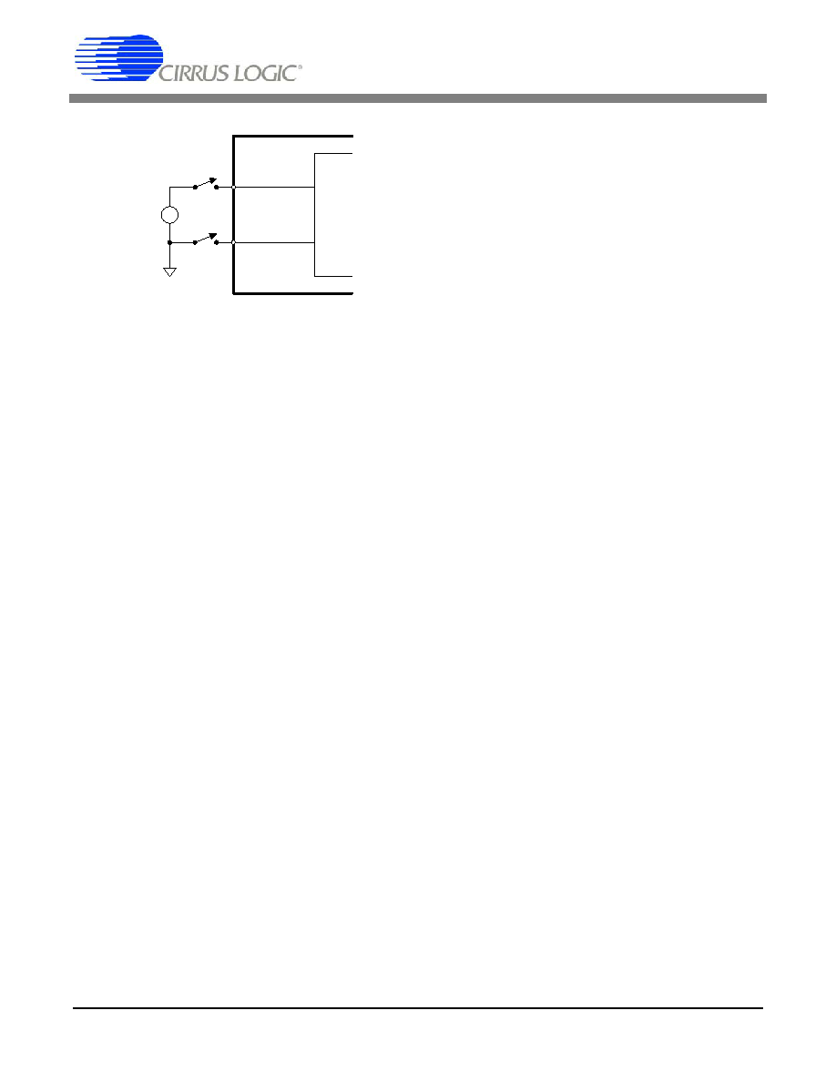
-
External
Connections
Full Scale
+
-
AIN+
AIN-
Figure 9. System Calibration of Gain.
相关PDF资料 |
PDF描述 |
|---|---|
| VE-J1F-EY | CONVERTER MOD DC/DC 72V 50W |
| GCM22DSXH | CONN EDGECARD 44POS DIP .156 SLD |
| CDB5368 | BOARD EVAL FOR CS5368 192KHZ ADC |
| VE-J1B-EY | CONVERTER MOD DC/DC 95V 50W |
| VE-J14-EY | CONVERTER MOD DC/DC 48V 50W |
相关代理商/技术参数 |
参数描述 |
|---|---|
| CDB5530U | 功能描述:数据转换 IC 开发工具 Eval Bd 24-Bit 1-Ch Low-Noise ADC RoHS:否 制造商:Texas Instruments 产品:Demonstration Kits 类型:ADC 工具用于评估:ADS130E08 接口类型:SPI 工作电源电压:- 6 V to + 6 V |
| CDB5532U | 功能描述:数据转换 IC 开发工具 Eval Bd 24Bit ADC w/ Ultra Low-Noise USB RoHS:否 制造商:Texas Instruments 产品:Demonstration Kits 类型:ADC 工具用于评估:ADS130E08 接口类型:SPI 工作电源电压:- 6 V to + 6 V |
| CDB5534U | 功能描述:数据转换 IC 开发工具 Eval Bd 24Bit ADC w/ Ultra Low-Noise USB RoHS:否 制造商:Texas Instruments 产品:Demonstration Kits 类型:ADC 工具用于评估:ADS130E08 接口类型:SPI 工作电源电压:- 6 V to + 6 V |
| CDB5534U-Z | 功能描述:EVAL BD 24-BIT ADCS W/ULTRALN PG 制造商:cirrus logic inc. 系列:- 零件状态:在售 A/D 转换器数:1 位数:24 采样率(每秒):3.84k 数据接口:串行 输入范围:±2.5 V 不同条件下的功率(典型值):35mW @ 3.84kSPS 使用的 IC/零件:CS5534 所含物品:板,电缆 标准包装:1 |
| CDB5540 | 制造商:Cirrus Logic 功能描述:EVAL BOARD FOR CS5540 - Bulk |
发布紧急采购,3分钟左右您将得到回复。