- 您现在的位置:买卖IC网 > PDF目录17026 > CDB5529 (Cirrus Logic Inc)EVAL BOARD FOR CS5529 PDF资料下载
参数资料
| 型号: | CDB5529 |
| 厂商: | Cirrus Logic Inc |
| 文件页数: | 9/31页 |
| 文件大小: | 0K |
| 描述: | EVAL BOARD FOR CS5529 |
| 标准包装: | 1 |
| ADC 的数量: | 1 |
| 位数: | 16 |
| 采样率(每秒): | 303 |
| 数据接口: | 串行 |
| 输入范围: | ±2.5 V |
| 在以下条件下的电源(标准): | 2.6mW @ 2.5V |
| 工作温度: | -40°C ~ 85°C |
| 已用 IC / 零件: | CS5529 |
| 已供物品: | 板,线缆,磁盘 |
| 产品目录页面: | 755 (CN2011-ZH PDF) |
| 相关产品: | CS5529-ASZR-ND - IC ADC 16BIT W/6BIT LATCH 20SSOP 598-1110-5-ND - IC ADC 16BIT W/6BIT LATCH 20SSOP |
| 其它名称: | 598-1015 |
第1页第2页第3页第4页第5页第6页第7页第8页当前第9页第10页第11页第12页第13页第14页第15页第16页第17页第18页第19页第20页第21页第22页第23页第24页第25页第26页第27页第28页第29页第30页第31页
CS5529
DS246F5
17
Port Flag
The port flag bit in the configuration register allows
the user to select the mode in which conversions
will be presented to the serial port. With the port
flag bit cleared, the user must read the conversion
data register. With the port flag bit set to logic 1, the
user can read the conversion data from the serial
port by first issuing the NULL command to clear
the SDO flag and then issuing 24 SCLKs to read
the conversion word.
Calibration
Calibration is used to set the zero and gain slope of
the ADC’s transfer function. The calibration con-
trol bits in the configuration register allow the user
to perform either self calibration or system calibra-
tion.
The offset and gain calibration steps each take one
conversion cycle to complete. At the end of the cal-
ibration step, the calibration control bits will be set
back to logic 0, and the DF (Done Flag) bit will be
set to a logic 1. For the combination self-calibration
(CC2-CC0= 011; offset calibration followed by
gain calibration), the calibration will take two con-
version cycles to complete and will set the DF bit
after the gain calibration is completed.
Note:
1) The DF bit will be cleared any time the data
register, the offset register, the gain register,
or the setup register is read. Reading the
configuration register alone will not clear the
DF bit.
2) After the CS5529 is reset, the converter is
functional and can perform measurements
without being calibrated. In this case, the
converter will utilize the initialized values of
the on-chip registers (Gain = 1.0, Offset = 0.0)
to calculate output words. Any initial offset
and gain errors in the internal circuitry of the
chip will remain.
Calibration Registers
The offset calibration result is stored in the offset
register. The result is used during the conversion
process to nullify offset errors. One LSB in the off-
set register is 2-24 proportion of the input span (bi-
polar span is 2 times the unipolar span). The MSB
in the offset register determines if the offset to be
trimmed is positive or negative (0 positive, 1 nega-
tive). The converter can typically trim ±50 percent
of the input span. Refer to the following Offset
Register and Gain Register descriptions for details.
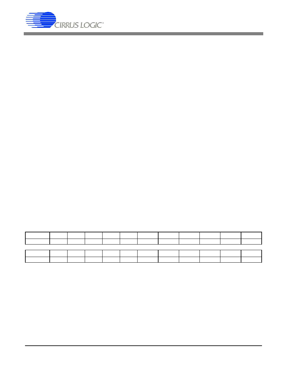
Offset Register
One LSB represents 2-24 proportion of the input span (bipolar span is 2 times unipolar span).
Offset and data word bits align by MSB (bit MSB-4 of offset register changes bit MSB-4 of data). After reset, all bits
are ‘0’.
23(MSB)
22
21
20
19
18
17
16
15
14
13
12
Sign
2-2
2-3
2-4
2-5
2-6
2-7
2-8
2-9
2-10
2-11
2-12
0
00000
0
11
10
9876
5
4
3
2
1
0
2-13
2-14
2-15
2-16
2-17
2-18
2-19
2-20
2-21
2-22
2-23
2-24
0
00000
0
相关PDF资料 |
PDF描述 |
|---|---|
| VE-J1F-EY | CONVERTER MOD DC/DC 72V 50W |
| GCM22DSXH | CONN EDGECARD 44POS DIP .156 SLD |
| CDB5368 | BOARD EVAL FOR CS5368 192KHZ ADC |
| VE-J1B-EY | CONVERTER MOD DC/DC 95V 50W |
| VE-J14-EY | CONVERTER MOD DC/DC 48V 50W |
相关代理商/技术参数 |
参数描述 |
|---|---|
| CDB5530U | 功能描述:数据转换 IC 开发工具 Eval Bd 24-Bit 1-Ch Low-Noise ADC RoHS:否 制造商:Texas Instruments 产品:Demonstration Kits 类型:ADC 工具用于评估:ADS130E08 接口类型:SPI 工作电源电压:- 6 V to + 6 V |
| CDB5532U | 功能描述:数据转换 IC 开发工具 Eval Bd 24Bit ADC w/ Ultra Low-Noise USB RoHS:否 制造商:Texas Instruments 产品:Demonstration Kits 类型:ADC 工具用于评估:ADS130E08 接口类型:SPI 工作电源电压:- 6 V to + 6 V |
| CDB5534U | 功能描述:数据转换 IC 开发工具 Eval Bd 24Bit ADC w/ Ultra Low-Noise USB RoHS:否 制造商:Texas Instruments 产品:Demonstration Kits 类型:ADC 工具用于评估:ADS130E08 接口类型:SPI 工作电源电压:- 6 V to + 6 V |
| CDB5534U-Z | 功能描述:EVAL BD 24-BIT ADCS W/ULTRALN PG 制造商:cirrus logic inc. 系列:- 零件状态:在售 A/D 转换器数:1 位数:24 采样率(每秒):3.84k 数据接口:串行 输入范围:±2.5 V 不同条件下的功率(典型值):35mW @ 3.84kSPS 使用的 IC/零件:CS5534 所含物品:板,电缆 标准包装:1 |
| CDB5540 | 制造商:Cirrus Logic 功能描述:EVAL BOARD FOR CS5540 - Bulk |
发布紧急采购,3分钟左右您将得到回复。