- 您现在的位置:买卖IC网 > PDF目录378829 > CH7303 (Electronic Theatre Controls, Inc.) Chrontel CH7303 HDTV / DVI Encoder PDF资料下载
参数资料
| 型号: | CH7303 |
| 厂商: | Electronic Theatre Controls, Inc. |
| 英文描述: | Chrontel CH7303 HDTV / DVI Encoder |
| 中文描述: | 昆泰CH7303的HDTV / DVI译码器 |
| 文件页数: | 4/15页 |
| 文件大小: | 330K |
| 代理商: | CH7303 |
CHRONTEL
CH7303
4
209-0000-031
Rev. 0.4,
8/26/2002
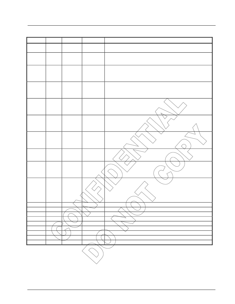
Table 1: Pin Description (contd.)
Pin #
# Pins
28, 27
2
Type
Symbol
TDC2,
TDC2*
TLC,
TLC*
Description
Out
DVI Data Channel 2 Outputs
These pins provide the DVI differential outputs for data channel 2 (red).
DVI Clock Outputs
These pins provide the differential clock output for the DVI interface
corresponding to data on the TDC[0:2] outputs.
Current Set Resistor Input
This pin sets the DAC current. A 140 ohm resistor should be connected
between this pin and DAC ground (pins 34 and 40) using short and wide
traces.
Luma / Green Output
This pin outputs a selectable video signal. The output is designed to drive a
75ohm doubly terminated load. The output can be selected to be the
luminance component of YprPb or Green.
Red / Pr Output
This pin outputs a selectable video signal. The output is designed to drive a
75ohm doubly terminated load. The output can be selected to be the Pr
component of YPrPb or red.
Blue / Pb Output
This pin outputs a selectable video signal. The output is designed to drive a
75ohm doubly terminated load. The output can be selected to be the Pb
component of YPrPb or blue.
VSYNC
By programming BCO register, a
buffered version of VGA vertical sync
can be acquired from this pin . This output pin can also provide a buffered
clock output, driven by the DVDD supply
.
Horizontal Sync Output
A buffered version of VGA horizontal sync can be acquired from this pin
via DC register)
D[14] - D[0]
Data[14] through Data[0] Inputs
These pins accept the 15 data inputs from a digital video port of a graphics
controller. The levels are 0 to VDDV, and the VREF signal is used as the
threshold level.
XCLK,
XCLK*
These inputs form a differential clock signal input to the CH7303 for use
with the H, V, DE and D[14:0] data. If differential clocks are not available,
the XCLK* input should be connected to VREF.
The clock polarity used can be selected using the MCP control bit.
DVDD
Digital Supply Voltage
(3.3V)
DGND
Digital Ground
VDDV
I/O Supply Voltage
(1.1V to 3.3V)
TVDD
DVI Transmitter Supply Voltage
(3.3V)
TGND
DVI Transmitter Ground
AVDD
PLL Supply Voltage
(3.3V)
AGND
PLL Ground
VDD
DAC Supply Voltage
(3.3V)
GND
DAC Ground
30, 31
2
Out
35
1
In
ISET
37
1
Out
Y/G
(DAC1)
38
1
Out
R/Pr
(DAC2)
39
1
Out
B/Pb
(DAC0)
47
1
Out
VSYNC
48
1
Out
HSYNC
50 -55,
58 –63,
42, 43, 46
15
In/Out
57, 56
2
In
External Clock Inputs
1, 12, 49
6, 11, 64
45
23, 29
20, 26, 32 3
18, 44
16, 17, 41 3
33
34, 40
3
3
1
2
Power
Power
Power
Power
Power
Power
Power
Power
Power
2
1
2
相关PDF资料 |
PDF描述 |
|---|---|
| CH8398A | TRUE-COLOR CHRONDAC WITH 16-BIT INTERFACE |
| CHF1206CNT | 20 W Power RF Chip Termination |
| CHF1206CNT500LY | 20 W Power RF Chip Termination |
| CHF1206CNT500LZ | 20 W Power RF Chip Termination |
| CHF1206CNT500LX | 20 W Power RF Chip Termination |
相关代理商/技术参数 |
参数描述 |
|---|---|
| CH7317A-TF | 制造商:CHRONTEL 功能描述:SERIAL INPUT LOADING, DAC WITH PROGRAMMABLE PLL, PQFP64 |
| CH731UPT | 制造商:CHENMKO 制造商全称:Chenmko Enterprise Co. Ltd. 功能描述:SCHOTTKY BARRIER DIODE VOLTAGE 40 Volts CURRENT 0.03 Ampere |
| CH732 | 制造商:Thomas & Betts 功能描述: |
| CH732MV | 制造商:Thomas & Betts 功能描述:B32 DBL LOCK SYS 1XPG29-1 |
| CH740H-40PT | 制造商:CHENMKO 制造商全称:Chenmko Enterprise Co. Ltd. 功能描述:SCHOTTKY BARRIER DIODE VOLTAGE 40 Volts CURRENT 0.04 Ampere |
发布紧急采购,3分钟左右您将得到回复。