- 您现在的位置:买卖IC网 > PDF目录378829 > CH7303 (Electronic Theatre Controls, Inc.) Chrontel CH7303 HDTV / DVI Encoder PDF资料下载
参数资料
| 型号: | CH7303 |
| 厂商: | Electronic Theatre Controls, Inc. |
| 英文描述: | Chrontel CH7303 HDTV / DVI Encoder |
| 中文描述: | 昆泰CH7303的HDTV / DVI译码器 |
| 文件页数: | 7/15页 |
| 文件大小: | 330K |
| 代理商: | CH7303 |
CHRONTEL
CH7303
209-0000-031
Rev. 0.4,
8/26/2002
7
2.3.2
The graphics controller interface can operate at a variable voltage level controlled by the voltage on the
VDDV
pin. This
should be set to the maximum voltage of the interface (typically 3.3V or adjustable between 1.1 and 1.8V). The VREF
pin is the voltage reference for the data, date enable, clock and sync inputs and must be tied to VDDV/2. This is typically
done using a resistor divider.
2.3.3
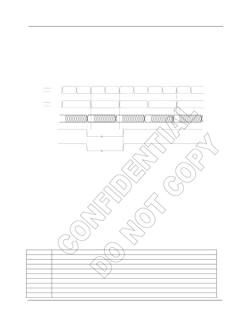
Input Clock and Data Timing Diagram
Figure 3 below shows the timing diagram for input data and clocks. The first XCLK/XCLK* waveform represents the
input clock for single edge transfer (SDR) methods. The second XCLK/XCLK* waveform represents the input clock for
the dual edge transfer (DDR) method. The timing requirements are given in section
Error! Reference source not
found.
.
XCLK/
XCLK*
Interface Voltage Levels
D[11:0]
H
V
XCLK/
XCLK*
Figure 3: Clock, Data and Interface Timing
2.3.4
The de-skew feature allows adjustment of the input setup and hold time. The input data D[14:0] can be latched slightly
before or after the latching edge of XCLK depending on the amount of the de-skew. Note that the XCLK is not changed,
only the time at which the data is latch relative to XCLK. .The de-skew is controlled using the XCMD[3:0] bits located
in CH7303 register. The delay t
CD
between clock and data is given by the following formula:
t
CD
= - XCMD[3:0] * t
STEP
for 0
≤
XCMD[3:0]
≤
7
t
CD
= (XCMD[3:0] – 8) * t
STEP
for 8
≤
XCMD[3:0]
≤
15
where XCMD is a number between 0 and 15 represented as a binary code
t
STEP
is the adjustment increment
2.3.5
Input Data Formats
The CH7303 supports 9 different multiplexed data formats, each of which can be used with a 1X clock latching data on
both clock edges, or a 2X clock latching data with a single edge (rising or falling depending on the value of the MCP bit
– rising refers to a rising edge on the XCLK signal, a falling edge on the XCLK* signal). The input data formats are
(IDF[2:0]):
IDF
Description
0
12-bit multiplexed RGB input (24-bit color), (multiplex scheme 1)
1
12-bit multiplexed RGB input (24-bit color), (multiplex scheme 2)
2
8-bit multiplexed RGB input (16-bit color, 565)
3
8-bit multiplexed RGB input (15-bit color, 555)
4
8-bit multiplexed YCrCb input (24-bit color), (Y, Cr and Cb are multiplexed)
5
12-bit multiplexed RGB input (24-bit color), (multiplex scheme A3 - edge-pair)
6
15-bit multiplexed RGB input (30-bit color), (multiplex scheme B1 - half-half mode)
7
15-bit multiplexed RGB input (30-bit color), (multiplex scheme B2 - half-color mode)
8
15-bit multiplexed RGB input (30-bit color), (multiplex scheme B3 - edge pair mode)
Data De-skew Feature
相关PDF资料 |
PDF描述 |
|---|---|
| CH8398A | TRUE-COLOR CHRONDAC WITH 16-BIT INTERFACE |
| CHF1206CNT | 20 W Power RF Chip Termination |
| CHF1206CNT500LY | 20 W Power RF Chip Termination |
| CHF1206CNT500LZ | 20 W Power RF Chip Termination |
| CHF1206CNT500LX | 20 W Power RF Chip Termination |
相关代理商/技术参数 |
参数描述 |
|---|---|
| CH7317A-TF | 制造商:CHRONTEL 功能描述:SERIAL INPUT LOADING, DAC WITH PROGRAMMABLE PLL, PQFP64 |
| CH731UPT | 制造商:CHENMKO 制造商全称:Chenmko Enterprise Co. Ltd. 功能描述:SCHOTTKY BARRIER DIODE VOLTAGE 40 Volts CURRENT 0.03 Ampere |
| CH732 | 制造商:Thomas & Betts 功能描述: |
| CH732MV | 制造商:Thomas & Betts 功能描述:B32 DBL LOCK SYS 1XPG29-1 |
| CH740H-40PT | 制造商:CHENMKO 制造商全称:Chenmko Enterprise Co. Ltd. 功能描述:SCHOTTKY BARRIER DIODE VOLTAGE 40 Volts CURRENT 0.04 Ampere |
发布紧急采购,3分钟左右您将得到回复。