- 您现在的位置:买卖IC网 > Datasheet目录319 > COP8SG-EPU (National Semiconductor)BOARD PROTOTYPE/TARGET COP8 Datasheet资料下载
参数资料
| 型号: | COP8SG-EPU |
| 厂商: | National Semiconductor |
| 文件页数: | 24/55页 |
| 文件大小: | 0K |
| 描述: | BOARD PROTOTYPE/TARGET COP8 |
| 标准包装: | 1 |
| 系列: | COP8™ |
| 类型: | MCU |
| 适用于相关产品: | Cop 8 |
| 所含物品: | 板 |
| 相关产品: | COP8SGR728M7-ND - MCU 8BIT CMOS ROM OTP 28-SOIC COP8SGR744V8-ND - IC MCU 8BIT CMOS OTP 44PLCC COP8SGR728N8/NOPB-ND - IC MCU 8BIT CMOS OTP 28DIP COP8SGR728M8-ND - IC MCU 8BIT CMOS OTP 28SOIC COP8SGE7VEJ8-ND - IC MCU 8BIT CMOS OTP 44LQFP COP8SGE744V8/NOPB-ND - IC MCU 8BIT CMOS OTP 44PLCC COP8SGE728N8-ND - IC MCU 8BIT CMOS OTP 28DIP COP8SGE728M8/NOPB-ND - IC MCU 8BIT CMOS OTP 28SOIC |
第1页第2页第3页第4页第5页第6页第7页第8页第9页第10页第11页第12页第13页第14页第15页第16页第17页第18页第19页第20页第21页第22页第23页当前第24页第25页第26页第27页第28页第29页第30页第31页第32页第33页第34页第35页第36页第37页第38页第39页第40页第41页第42页第43页第44页第45页第46页第47页第48页第49页第50页第51页第52页第53页第54页第55页
�� �
�
�Power� Save� Modes�
�(Continued)�
�device� will� first� execute� the� Timer� T0� interrupt� service� routine�
�and� then� return� to� the� instruction� following� the� “Enter� Idle�
�micro-controller� in� this� mode� of� operation� are� typically�
�around� 30%� of� normal� power� requirement� of� the� microcon-�
�troller.�
�As� with� the� HALT� mode,� the� device� can� be� returned� to� nor-�
�mal� operation� with� a� reset,� or� with� a� Multi-Input� Wakeup� from�
�the� L� Port.� Alternately,� the� microcontroller� resumes� normal�
�operation� from� the� IDLE� mode� when� the� thirteenth� bit� (repre-�
�senting� 4.096� ms� at� internal� clock� frequency� of� 10� MHz,� t� c� =�
�1� μs)� of� the� IDLE� Timer� toggles.�
�This� toggle� condition� of� the� thirteenth� bit� of� the� IDLE� Timer�
�T0� is� latched� into� the� T0PND� pending� flag.�
�The� user� has� the� option� of� being� interrupted� with� a� transition�
�on� the� thirteenth� bit� of� the� IDLE� Timer� T0.� The� interrupt� can�
�be� enabled� or� disabled� via� the� T0EN� control� bit.� Setting� the�
�T0EN� flag� enables� the� interrupt� and� vice� versa.�
�The� user� can� enter� the� IDLE� mode� with� the� Timer� T0� inter-�
�Mode”� instruction.�
�Alternatively,� the� user� can� enter� the� IDLE� mode� with� the�
�IDLE� Timer� T0� interrupt� disabled.� In� this� case,� the� device� will�
�resume� normal� operation� with� the� instruction� immediately�
�following� the� “Enter� IDLE� Mode”� instruction.�
�Note:� It� is� necessary� to� program� two� NOP� instructions� following� both� the� set�
�HALT� mode� and� set� IDLE� mode� instructions.� These� NOP� instructions�
�are� necessary� to� allow� clock� resynchronization� following� the� HALT� or�
�IDLE� modes.�
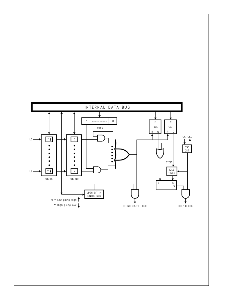
�Multi-Input� Wakeup�
�The� Multi-Input� Wakeup� feature� is� ued� to� return� (wakeup)� the�
�device� from� either� the� HALT� or� IDLE� modes.� Alternately�
�Multi-Input� Wakeup/Interrupt� feature� may� also� be� used� to�
�generate� up� to� 8� edge� selectable� external� interrupts.�
�Figure� 11� shows� the� Multi-Input� Wakeup� logic.�
�rupt� enabled.� In� this� case,� when� the� T0PND� bit� gets� set,� the�
�DS012829-13�
�FIGURE� 11.� Multi-Input� Wake� Up� Logic�
�The� Multi-Input� Wakeup� feature� utilizes� the� L� Port.� The� user�
�selects� which� particular� L� port� bit� (or� combination� of� L� Port�
�bits)� will� cause� the� device� to� exit� the� HALT� or� IDLE� modes.�
�The� selection� is� done� through� the� Register� WKEN.� The� Reg-�
�ister� WKEN� is� an� 8-bit� read/write� register,� which� contains� a�
�control� bit� for� every� L� port� bit.� Setting� a� particular� WKEN� bit�
�enables� a� Wakeup� from� the� associated� L� port� pin.�
�The� user� can� select� whether� the� trigger� condition� on� the� se-�
�lected� L� Port� pin� is� going� to� be� either� a� positive� edge� (low� to�
�high� transition)� or� a� negative� edge� (high� to� low� transition).�
�This� selection� is� made� via� the� Register� WKEDG,� which� is� an�
�8-bit� control� register� with� a� bit� assigned� to� each� L� Port� pin.�
�Setting� the� control� bit� will� select� the� trigger� condition� to� be� a�
�negative� edge� on� that� particular� L� Port� pin.� Resetting� the� bit�
�selects� the� trigger� condition� to� be� a� positive� edge.� Changing�
�23�
�an� edge� select� entails� several� steps� in� order� to� avoid� a�
�Wakeup� condition� as� a� result� of� the� edge� change.� First,� the�
�associated� WKEN� bit� should� be� reset,� followed� by� the� edge�
�select� change� in� WKEDG.� Next,� the� associated� WKPND� bit�
�should� be� cleared,� followed� by� the� associated� WKEN� bit� be-�
�ing� re-enabled.�
�An� example� may� serve� to� clarify� this� procedure.� Suppose� we�
�wish� to� change� the� edge� select� from� positive� (low� going� high)�
�to� negative� (high� going� low)� for� L� Port� bit� 5,� where� bit� 5� has�
�previously� been� enabled� for� an� input� interrupt.� The� program�
�would� be� as� follows:�
�RBIT� 5,� WKEN� ;� Disable� MIWU�
�SBIT� 5,� WKEDG� ;� Change� edge� polarity�
�RBIT� 5,� WKPND� ;� Reset� pending� flag�
�SBIT� 5,� WKEN� ;� Enable� MIWU�
�www.national.com�
�相关PDF资料 |
PDF描述 |
|---|---|
| CORE1553-DEV-KIT | KIT DEVELOPMENT FOR IP CORE1553 |
| CP131-AG | LNR PWR SUP 5V 8A, +/-12V 1.7A |
| CPC1590P | MOSFET GATE DVR ISO 8-FLATPACK |
| CPC5002G | ISOLAT DGTL 3.75KVRMS 2CH 8-DIP |
| CPCI-D-3U-300C | PWR SUPLY DC/DC CPCI 300W 3UX8HP |
相关代理商/技术参数 |
参数描述 |
|---|---|
| COP8SGR728M7 | 功能描述:8位微控制器 -MCU RoHS:否 制造商:Silicon Labs 核心:8051 处理器系列:C8051F39x 数据总线宽度:8 bit 最大时钟频率:50 MHz 程序存储器大小:16 KB 数据 RAM 大小:1 KB 片上 ADC:Yes 工作电源电压:1.8 V to 3.6 V 工作温度范围:- 40 C to + 105 C 封装 / 箱体:QFN-20 安装风格:SMD/SMT |
| COP8SGR728M7/NOPB | 功能描述:8位微控制器 -MCU RoHS:否 制造商:Silicon Labs 核心:8051 处理器系列:C8051F39x 数据总线宽度:8 bit 最大时钟频率:50 MHz 程序存储器大小:16 KB 数据 RAM 大小:1 KB 片上 ADC:Yes 工作电源电压:1.8 V to 3.6 V 工作温度范围:- 40 C to + 105 C 封装 / 箱体:QFN-20 安装风格:SMD/SMT |
| COP8SGR728M8 | 功能描述:8位微控制器 -MCU RoHS:否 制造商:Silicon Labs 核心:8051 处理器系列:C8051F39x 数据总线宽度:8 bit 最大时钟频率:50 MHz 程序存储器大小:16 KB 数据 RAM 大小:1 KB 片上 ADC:Yes 工作电源电压:1.8 V to 3.6 V 工作温度范围:- 40 C to + 105 C 封装 / 箱体:QFN-20 安装风格:SMD/SMT |
| COP8SGR728M8/NOPB | 功能描述:8位微控制器 -MCU RoHS:否 制造商:Silicon Labs 核心:8051 处理器系列:C8051F39x 数据总线宽度:8 bit 最大时钟频率:50 MHz 程序存储器大小:16 KB 数据 RAM 大小:1 KB 片上 ADC:Yes 工作电源电压:1.8 V to 3.6 V 工作温度范围:- 40 C to + 105 C 封装 / 箱体:QFN-20 安装风格:SMD/SMT |
| COP8SGR728N8 | 功能描述:8位微控制器 -MCU RoHS:否 制造商:Silicon Labs 核心:8051 处理器系列:C8051F39x 数据总线宽度:8 bit 最大时钟频率:50 MHz 程序存储器大小:16 KB 数据 RAM 大小:1 KB 片上 ADC:Yes 工作电源电压:1.8 V to 3.6 V 工作温度范围:- 40 C to + 105 C 封装 / 箱体:QFN-20 安装风格:SMD/SMT |
发布紧急采购,3分钟左右您将得到回复。