- 您现在的位置:买卖IC网 > Datasheet目录319 > COP8SG-EPU (National Semiconductor)BOARD PROTOTYPE/TARGET COP8 Datasheet资料下载
参数资料
| 型号: | COP8SG-EPU |
| 厂商: | National Semiconductor |
| 文件页数: | 43/55页 |
| 文件大小: | 0K |
| 描述: | BOARD PROTOTYPE/TARGET COP8 |
| 标准包装: | 1 |
| 系列: | COP8™ |
| 类型: | MCU |
| 适用于相关产品: | Cop 8 |
| 所含物品: | 板 |
| 相关产品: | COP8SGR728M7-ND - MCU 8BIT CMOS ROM OTP 28-SOIC COP8SGR744V8-ND - IC MCU 8BIT CMOS OTP 44PLCC COP8SGR728N8/NOPB-ND - IC MCU 8BIT CMOS OTP 28DIP COP8SGR728M8-ND - IC MCU 8BIT CMOS OTP 28SOIC COP8SGE7VEJ8-ND - IC MCU 8BIT CMOS OTP 44LQFP COP8SGE744V8/NOPB-ND - IC MCU 8BIT CMOS OTP 44PLCC COP8SGE728N8-ND - IC MCU 8BIT CMOS OTP 28DIP COP8SGE728M8/NOPB-ND - IC MCU 8BIT CMOS OTP 28SOIC |
第1页第2页第3页第4页第5页第6页第7页第8页第9页第10页第11页第12页第13页第14页第15页第16页第17页第18页第19页第20页第21页第22页第23页第24页第25页第26页第27页第28页第29页第30页第31页第32页第33页第34页第35页第36页第37页第38页第39页第40页第41页第42页当前第43页第44页第45页第46页第47页第48页第49页第50页第51页第52页第53页第54页第55页
�� �
�
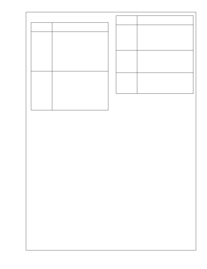
�Memory� Map�
�Address�
�S/ADD� REG�
�(Continued)�
�Contents�
�Address�
�S/ADD� REG�
�xxEC�
�Contents�
�Timer� T1� Autoload� Register� T1RA� Lower�
�Byte�
�xxD6�
�xxD7�
�xxD8�
�xxD9�
�xxDA�
�xxDB�
�xxDC�
�xxDD� to� xxDF�
�xxE0� to� xxE5�
�xxE6�
�xxE7�
�Port� G� Input� Pins� (Read� Only)�
�Port� I� Input� Pins� (Read� Only)� (Actually�
�reads� Port� F� input� pins)�
�Port� C� Data� Register�
�Port� C� Configuration� Register�
�Port� C� Input� Pins� (Read� Only)�
�Reserved� for� Port� C�
�Port� D�
�Reserved� for� Port� D�
�Reserved� for� EE� Control� Registers�
�Timer� T1� Autoload� Register� T1RB� Lower�
�Byte�
�Timer� T1� Autoload� Register� T1RB� Upper�
�Byte�
�xxED�
�xxEE�
�xxEF�
�xxF0� to� FB�
�xxFC�
�xxFD�
�xxFE�
�xxFF�
�0100–017F�
�0200–027F�
�0300–037F�
�Timer� T1� Autoload� Register� T1RA� Upper�
�Byte�
�CNTRL� Control� Register�
�PSW� Register�
�On-Chip� RAM� Mapped� as� Registers�
�X� Register�
�SP� Register�
�B� Register�
�S� Register�
�On-Chip� 128� RAM� Bytes�
�On-Chip� 128� RAM� Bytes� (Reads� as�
�undefined� data� on� COP8SGE)�
�On-Chip� 128� RAM� Bytes� (Reads� as�
�undefined� data� on� COP8SGE)�
�xxE8�
�xxE9�
�xxEA�
�xxEB�
�ICNTRL� Register�
�MICROWIRE/PLUS� Shift� Register�
�Timer� T1� Lower� Byte�
�Timer� T1� Upper� Byte�
�Note:� Reading� memory� locations� 0070H–007FH� (Segment� 0)� will� return� all�
�ones.� Reading� unused� memory� locations� 0080H–00AFH� (Segment� 0)�
�will� return� undefined� data.� Reading� memory� locations� from� other� Seg-�
�ments� (i.e.,� Segment� 2,� Segment� 3,� …� etc.)� will� return� undefined� data.�
�Addressing� Modes�
�There� are� ten� addressing� modes,� six� for� operand� addressing�
�TRANSFER� OF� CONTROL� ADDRESSING� MODES�
�and� four� for� transfer� of� control.�
�Relative�
�OPERAND� ADDRESSING� MODES�
�Register� Indirect�
�This� is� the� “normal”� addressing� mode.� The� operand� is� the�
�data� memory� addressed� by� the� B� pointer� or� X� pointer.�
�Register� Indirect� (with� auto� post� increment� or�
�decrement� of� pointer)�
�This� addressing� mode� is� used� with� the� LD� and� X� instruc-�
�tions.� The� operand� is� the� data� memory� addressed� by� the� B�
�pointer� or� X� pointer.� This� is� a� register� indirect� mode� that� au-�
�tomatically� post� increments� or� decrements� the� B� or� X� regis-�
�ter� after� executing� the� instruction.�
�Direct�
�The� instruction� contains� an� 8-bit� address� field� that� directly�
�points� to� the� data� memory� for� the� operand.�
�Immediate�
�The� instruction� contains� an� 8-bit� immediate� field� as� the� oper-�
�and.�
�Short� Immediate�
�This� addressing� mode� is� used� with� the� Load� B� Immediate� in-�
�struction.� The� instruction� contains� a� 4-bit� immediate� field� as�
�the� operand.�
�Indirect�
�This� addressing� mode� is� used� with� the� LAID� instruction.� The�
�contents� of� the� accumulator� are� used� as� a� partial� address�
�(lower� 8� bits� of� PC)� for� accessing� a� data� operand� from� the�
�program� memory.�
�www.national.com�
�42�
�This� mode� is� used� for� the� JP� instruction,� with� the� instruction�
�field� being� added� to� the� program� counter� to� get� the� new� pro-�
�gram� location.� JP� has� a� range� from� ?31� to� +32� to� allow� a�
�1-byte� relative� jump� (JP� +� 1� is� implemented� by� a� NOP� in-�
�struction).� There� are� no� “pages”� when� using� JP,� since� all� 15�
�bits� of� PC� are� used.�
�Absolute�
�This� mode� is� used� with� the� JMP� and� JSR� instructions,� with�
�the� instruction� field� of� 12� bits� replacing� the� lower� 12� bits� of�
�the� program� counter� (PC).� This� allows� jumping� to� any� loca-�
�tion� in� the� current� 4k� program� memory� segment.�
�Absolute� Long�
�This� mode� is� used� with� the� JMPL� and� JSRL� instructions,� with�
�the� instruction� field� of� 15� bits� replacing� the� entire� 15� bits� of�
�the� program� counter� (PC).� This� allows� jumping� to� any� loca-�
�tion� up� to� 32k� in� the� program� memory� space.�
�Indirect�
�This� mode� is� used� with� the� JID� instruction.� The� contents� of�
�the� accumulator� are� used� as� a� partial� address� (lower� 8� bits� of�
�PC)� for� accessing� a� location� in� the� program� memory.� The�
�contents� of� this� program� memory� location� serve� as� a� partial�
�address� (lower� 8� bits� of� PC)� for� the� jump� to� the� next� instruc-�
�tion.�
�Note:� The� VIS� is� a� special� case� of� the� Indirect� Transfer� of� Control� addressing�
�mode,� where� the� double� byte� vector� associated� with� the� interrupt� is�
�transferred� from� adjacent� addresses� in� the� program� memory� into� the�
�program� counter� (PC)� in� order� to� jump� to� the� associated� interrupt� ser-�
�vice� routine.�
�相关PDF资料 |
PDF描述 |
|---|---|
| CORE1553-DEV-KIT | KIT DEVELOPMENT FOR IP CORE1553 |
| CP131-AG | LNR PWR SUP 5V 8A, +/-12V 1.7A |
| CPC1590P | MOSFET GATE DVR ISO 8-FLATPACK |
| CPC5002G | ISOLAT DGTL 3.75KVRMS 2CH 8-DIP |
| CPCI-D-3U-300C | PWR SUPLY DC/DC CPCI 300W 3UX8HP |
相关代理商/技术参数 |
参数描述 |
|---|---|
| COP8SGR728M7 | 功能描述:8位微控制器 -MCU RoHS:否 制造商:Silicon Labs 核心:8051 处理器系列:C8051F39x 数据总线宽度:8 bit 最大时钟频率:50 MHz 程序存储器大小:16 KB 数据 RAM 大小:1 KB 片上 ADC:Yes 工作电源电压:1.8 V to 3.6 V 工作温度范围:- 40 C to + 105 C 封装 / 箱体:QFN-20 安装风格:SMD/SMT |
| COP8SGR728M7/NOPB | 功能描述:8位微控制器 -MCU RoHS:否 制造商:Silicon Labs 核心:8051 处理器系列:C8051F39x 数据总线宽度:8 bit 最大时钟频率:50 MHz 程序存储器大小:16 KB 数据 RAM 大小:1 KB 片上 ADC:Yes 工作电源电压:1.8 V to 3.6 V 工作温度范围:- 40 C to + 105 C 封装 / 箱体:QFN-20 安装风格:SMD/SMT |
| COP8SGR728M8 | 功能描述:8位微控制器 -MCU RoHS:否 制造商:Silicon Labs 核心:8051 处理器系列:C8051F39x 数据总线宽度:8 bit 最大时钟频率:50 MHz 程序存储器大小:16 KB 数据 RAM 大小:1 KB 片上 ADC:Yes 工作电源电压:1.8 V to 3.6 V 工作温度范围:- 40 C to + 105 C 封装 / 箱体:QFN-20 安装风格:SMD/SMT |
| COP8SGR728M8/NOPB | 功能描述:8位微控制器 -MCU RoHS:否 制造商:Silicon Labs 核心:8051 处理器系列:C8051F39x 数据总线宽度:8 bit 最大时钟频率:50 MHz 程序存储器大小:16 KB 数据 RAM 大小:1 KB 片上 ADC:Yes 工作电源电压:1.8 V to 3.6 V 工作温度范围:- 40 C to + 105 C 封装 / 箱体:QFN-20 安装风格:SMD/SMT |
| COP8SGR728N8 | 功能描述:8位微控制器 -MCU RoHS:否 制造商:Silicon Labs 核心:8051 处理器系列:C8051F39x 数据总线宽度:8 bit 最大时钟频率:50 MHz 程序存储器大小:16 KB 数据 RAM 大小:1 KB 片上 ADC:Yes 工作电源电压:1.8 V to 3.6 V 工作温度范围:- 40 C to + 105 C 封装 / 箱体:QFN-20 安装风格:SMD/SMT |
发布紧急采购,3分钟左右您将得到回复。