- 您现在的位置:买卖IC网 > Datasheet目录319 > COP8SG-EPU (National Semiconductor)BOARD PROTOTYPE/TARGET COP8 Datasheet资料下载
参数资料
| 型号: | COP8SG-EPU |
| 厂商: | National Semiconductor |
| 文件页数: | 41/55页 |
| 文件大小: | 0K |
| 描述: | BOARD PROTOTYPE/TARGET COP8 |
| 标准包装: | 1 |
| 系列: | COP8™ |
| 类型: | MCU |
| 适用于相关产品: | Cop 8 |
| 所含物品: | 板 |
| 相关产品: | COP8SGR728M7-ND - MCU 8BIT CMOS ROM OTP 28-SOIC COP8SGR744V8-ND - IC MCU 8BIT CMOS OTP 44PLCC COP8SGR728N8/NOPB-ND - IC MCU 8BIT CMOS OTP 28DIP COP8SGR728M8-ND - IC MCU 8BIT CMOS OTP 28SOIC COP8SGE7VEJ8-ND - IC MCU 8BIT CMOS OTP 44LQFP COP8SGE744V8/NOPB-ND - IC MCU 8BIT CMOS OTP 44PLCC COP8SGE728N8-ND - IC MCU 8BIT CMOS OTP 28DIP COP8SGE728M8/NOPB-ND - IC MCU 8BIT CMOS OTP 28SOIC |
第1页第2页第3页第4页第5页第6页第7页第8页第9页第10页第11页第12页第13页第14页第15页第16页第17页第18页第19页第20页第21页第22页第23页第24页第25页第26页第27页第28页第29页第30页第31页第32页第33页第34页第35页第36页第37页第38页第39页第40页当前第41页第42页第43页第44页第45页第46页第47页第48页第49页第50页第51页第52页第53页第54页第55页
�� �
�
�MICROWIRE/PLUS�
�(Continued)�
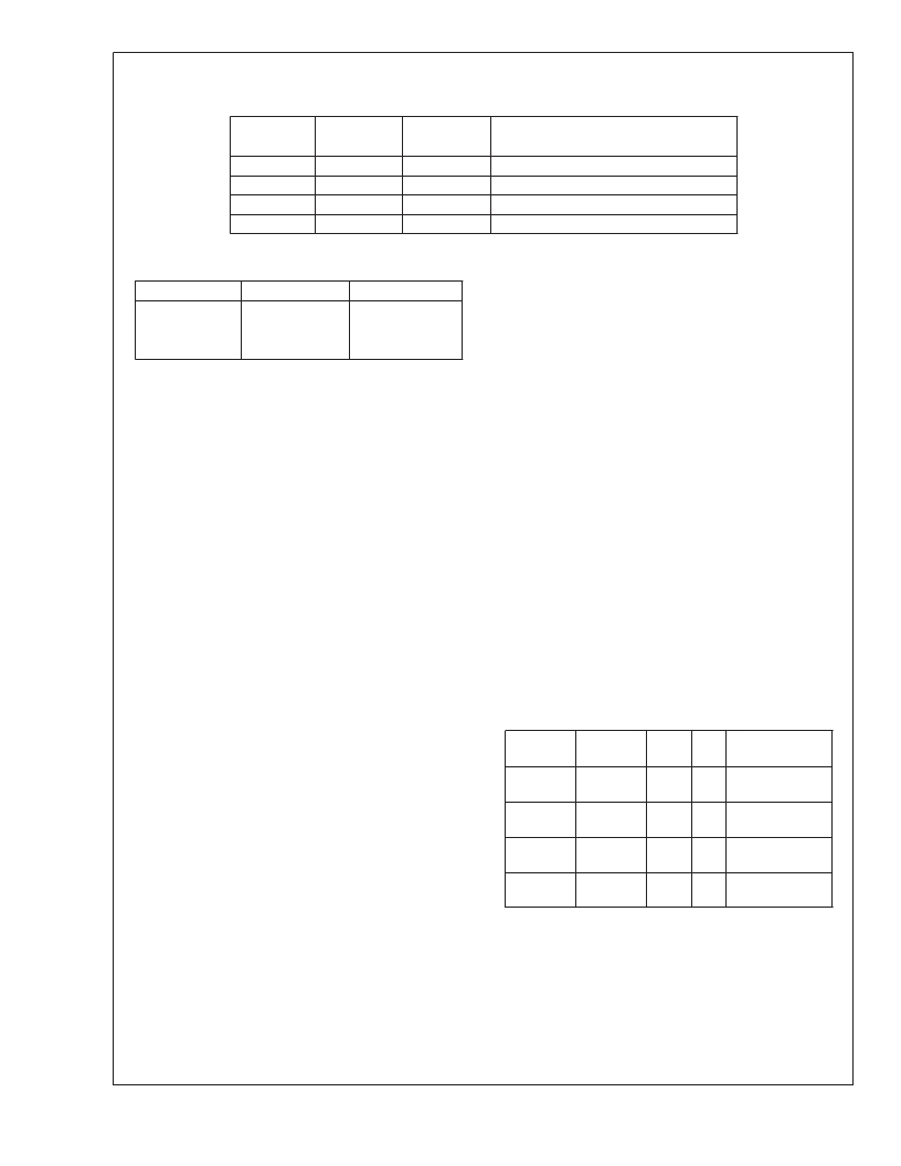
�TABLE� 8.� WATCHDOG� Service� Actions�
�Key�
�Data�
�Match�
�Don’t� Care�
�Mismatch�
�Don’t� Care�
�Window�
�Data�
�Match�
�Mismatch�
�Don’t� Care�
�Don’t� Care�
�Clock�
�Monitor�
�Match�
�Don’t� Care�
�Don’t� Care�
�Mismatch�
�Action�
�Valid� Service:� Restart� Service� Window�
�Error:� Generate� WATCHDOG� Output�
�Error:� Generate� WATCHDOG� Output�
�Error:� Generate� WATCHDOG� Output�
�TABLE� 9.� MICROWIRE/PLUS�
�Master� Mode� Clock� Select�
�onto� the� G� Port.� The� SK� pin� must� be� selected� as� an� input�
�and� the� SO� pin� is� selected� as� an� output� pin� by� setting� and� re-�
�SL1�
�0�
�0�
�SL0�
�0�
�1�
�SK�
�2� x� t� c�
�4� x� t� c�
�setting� the� appropriate� bits� in� the� Port� G� configuration� regis-�
�ter.� Table� 10� summarizes� the� settings� required� to� enter� the�
�Slave� mode� of� operation.�
�The� user� must� set� the� BUSY� flag� immediately� upon� entering�
�1�
�x� 8� x� t� c�
�Where� t� c� is� the� instruction� cycle� clock�
�the� Slave� mode.� This� will� ensure� that� all� data� bits� sent� by� the�
�Master� will� be� shifted� properly.� After� eight� clock� pulses� the�
�BUSY� flag� will� be� cleared� and� the� sequence� may� be� re-�
�MICROWIRE/PLUS� OPERATION�
�Setting� the� BUSY� bit� in� the� PSW� register� causes� the�
�MICROWIRE/PLUS� to� start� shifting� the� data.� It� gets� reset�
�when� eight� data� bits� have� been� shifted.� The� user� may� reset�
�the� BUSY� bit� by� software� to� allow� less� than� 8� bits� to� shift.� If�
�enabled,� an� interrupt� is� generated� when� eight� data� bits� have�
�been� shifted.� The� device� may� enter� the� MICROWIRE/PLUS�
�mode� either� as� a� Master� or� as� a� Slave.� Figure� 20� shows� how�
�two� microcontroller� devices� and� several� peripherals� may� be�
�interconnected� using� the� MICROWIRE/PLUS� arrangements.�
�Warning:�
�The� SIO� register� should� only� be� loaded� when� the� SK� clock� is�
�low.� Loading� the� SIO� register� while� the� SK� clock� is� high� will�
�result� in� undefined� data� in� the� SIO� register.� SK� clock� is� nor-�
�mally� low� when� not� shifting.�
�Setting� the� BUSY� flag� when� the� input� SK� clock� is� high� in� the�
�MICROWIRE/PLUS� slave� mode� may� cause� the� current� SK�
�clock� for� the� SIO� shift� register� to� be� narrow.� For� safety,� the�
�BUSY� flag� should� only� be� set� when� the� input� SK� clock� is� low.�
�MICROWIRE/PLUS� Master� Mode� Operation�
�peated.�
�Alternate� SK� Phase� Operation�
�The� device� allows� either� the� normal� SK� clock� or� an� alternate�
�phase� SK� clock� to� shift� data� in� and� out� of� the� SIO� register.� In�
�both� the� modes� the� SK� is� normally� low.� In� the� normal� mode�
�data� is� shifted� in� on� the� rising� edge� of� the� SK� clock� and� the�
�data� is� shifted� out� on� the� falling� edge� of� the� SK� clock.� The�
�SIO� register� is� shifted� on� each� falling� edge� of� the� SK� clock.�
�In� the� alternate� SK� phase� operation,� data� is� shifted� in� on� the�
�falling� edge� of� the� SK� clock� and� shifted� out� on� the� rising� edge�
�of� the� SK� clock.�
�A� control� flag,� SKSEL,� allows� either� the� normal� SK� clock� or�
�the� alternate� SK� clock� to� be� selected.� Resetting� SKSEL�
�causes� the� MICROWIRE/PLUS� logic� to� be� clocked� from� the�
�normal� SK� signal.� Setting� the� SKSEL� flag� selects� the� alter-�
�nate� SK� clock.� The� SKSEL� is� mapped� into� the� G6� configura-�
�tion� bit.� The� SKSEL� flag� will� power� up� in� the� reset� condition,�
�selecting� the� normal� SK� signal.�
�TABLE� 10.� MICROWIRE/PLUS� Mode� Settings�
�This� table� assumes� that� the� control� flag� MSEL� is� set.�
�In� the� MICROWIRE/PLUS� Master� mode� of� operation� the�
�shift� clock� (SK)� is� generated� internally� by� the� device.� The� MI-�
�CROWIRE� Master� always� initiates� all� data� exchanges.� The�
�MSEL� bit� in� the� CNTRL� register� must� be� set� to� enable� the�
�SO� and� SK� functions� onto� the� G� Port.� The� SO� and� SK� pins�
�must� also� be� selected� as� outputs� by� setting� appropriate� bits�
�in� the� Port� G� configuration� register.� Table� 10� summarizes� the�
�bit� settings� required� for� Master� mode� of� operation.�
�G4� (SO)�
�Config.� Bit�
�1�
�0�
�1�
�G5� (SK)�
�Config.� Bit�
�1�
�1�
�0�
�G4�
�Fun.�
�SO�
�TRI-�
�STATE�
�SO�
�G5�
�Fun.�
�Int.�
�SK�
�Int.�
�SK�
�Ext.�
�Operation�
�MICROWIRE/PLUS�
�Master�
�MICROWIRE/PLUS�
�Master�
�MICROWIRE/PLUS�
�SK�
�Slave�
�MICROWIRE/PLUS� Slave� Mode� Operation�
�In� the� MICROWIRE/PLUS� Slave� mode� of� operation� the� SK�
�clock� is� generated� by� an� external� source.� Setting� the� MSEL�
�0�
�0�
�TRI-�
�STATE�
�Ext.�
�SK�
�MICROWIRE/PLUS�
�Slave�
�bit� in� the� CNTRL� register� enables� the� SO� and� SK� functions�
�www.national.com�
�40�
�相关PDF资料 |
PDF描述 |
|---|---|
| CORE1553-DEV-KIT | KIT DEVELOPMENT FOR IP CORE1553 |
| CP131-AG | LNR PWR SUP 5V 8A, +/-12V 1.7A |
| CPC1590P | MOSFET GATE DVR ISO 8-FLATPACK |
| CPC5002G | ISOLAT DGTL 3.75KVRMS 2CH 8-DIP |
| CPCI-D-3U-300C | PWR SUPLY DC/DC CPCI 300W 3UX8HP |
相关代理商/技术参数 |
参数描述 |
|---|---|
| COP8SGR728M7 | 功能描述:8位微控制器 -MCU RoHS:否 制造商:Silicon Labs 核心:8051 处理器系列:C8051F39x 数据总线宽度:8 bit 最大时钟频率:50 MHz 程序存储器大小:16 KB 数据 RAM 大小:1 KB 片上 ADC:Yes 工作电源电压:1.8 V to 3.6 V 工作温度范围:- 40 C to + 105 C 封装 / 箱体:QFN-20 安装风格:SMD/SMT |
| COP8SGR728M7/NOPB | 功能描述:8位微控制器 -MCU RoHS:否 制造商:Silicon Labs 核心:8051 处理器系列:C8051F39x 数据总线宽度:8 bit 最大时钟频率:50 MHz 程序存储器大小:16 KB 数据 RAM 大小:1 KB 片上 ADC:Yes 工作电源电压:1.8 V to 3.6 V 工作温度范围:- 40 C to + 105 C 封装 / 箱体:QFN-20 安装风格:SMD/SMT |
| COP8SGR728M8 | 功能描述:8位微控制器 -MCU RoHS:否 制造商:Silicon Labs 核心:8051 处理器系列:C8051F39x 数据总线宽度:8 bit 最大时钟频率:50 MHz 程序存储器大小:16 KB 数据 RAM 大小:1 KB 片上 ADC:Yes 工作电源电压:1.8 V to 3.6 V 工作温度范围:- 40 C to + 105 C 封装 / 箱体:QFN-20 安装风格:SMD/SMT |
| COP8SGR728M8/NOPB | 功能描述:8位微控制器 -MCU RoHS:否 制造商:Silicon Labs 核心:8051 处理器系列:C8051F39x 数据总线宽度:8 bit 最大时钟频率:50 MHz 程序存储器大小:16 KB 数据 RAM 大小:1 KB 片上 ADC:Yes 工作电源电压:1.8 V to 3.6 V 工作温度范围:- 40 C to + 105 C 封装 / 箱体:QFN-20 安装风格:SMD/SMT |
| COP8SGR728N8 | 功能描述:8位微控制器 -MCU RoHS:否 制造商:Silicon Labs 核心:8051 处理器系列:C8051F39x 数据总线宽度:8 bit 最大时钟频率:50 MHz 程序存储器大小:16 KB 数据 RAM 大小:1 KB 片上 ADC:Yes 工作电源电压:1.8 V to 3.6 V 工作温度范围:- 40 C to + 105 C 封装 / 箱体:QFN-20 安装风格:SMD/SMT |
发布紧急采购,3分钟左右您将得到回复。