参数资料
| 型号: | CS5376A-IQZ |
| 厂商: | Cirrus Logic Inc |
| 文件页数: | 1/49页 |
| 文件大小: | 0K |
| 描述: | IC FILTER DGTL MULTI-CH 64-TQFP |
| 标准包装: | 160 |
| 滤波器类型: | 数字 |
| 滤波器数: | 4 |
| 滤波器阶数: | 2nd |
| 电源电压: | 3 V ~ 5 V |
| 安装类型: | 表面贴装 |
| 封装/外壳: | 64-LQFP |
| 供应商设备封装: | 64-TQFP(10x10) |
| 包装: | 管件 |
| 配用: | 598-1778-ND - EVALUATION BOARD FOR CS5376 |
当前第1页第2页第3页第4页第5页第6页第7页第8页第9页第10页第11页第12页第13页第14页第15页第16页第17页第18页第19页第20页第21页第22页第23页第24页第25页第26页第27页第28页第29页第30页第31页第32页第33页第34页第35页第36页第37页第38页第39页第40页第41页第42页第43页第44页第45页第46页第47页第48页第49页
Copyright
Cirrus Logic, Inc. 2008
(All Rights Reserved)
CS5376A
Low-power, Multi-channel Decimation Filter
Features
1- to 4-channel Digital Decimation Filter
Multiple On-chip FIR and IIR Coefficient Sets
Programmable Coefficients for Custom Filters
Synchronous Operation
Selectable Output Word Rate
4000, 2000, 1000, 500, 333, 250 SPS
200, 125, 100, 50, 40, 25, 20, 10, 5, 1 SPS
Digital Gain and Offset Corrections
Test DAC Bit-stream Generator
Digital Sine Wave Output
Time Break Controller, General Purpose I/O
Secondary SPI Port, Boundary Scan JTAG
Microcontroller or EEPROM Configuration
Small-footprint, 64-pin TQFP Package
Low Power Consumption
9 mW per Channel at 500 SPS
Flexible Power Supplies
I/O Interface: 3.3 V or 5.0 V
Digital Logic Core: 3.0 V, 3.3 V or 5.0 V
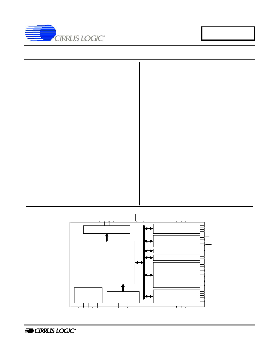
Description
The CS5376A is a multi-function digital filter utilizing a
low-power signal processing architecture to achieve ef-
ficient filtering for up to four
Σ modulators. By
combining the CS5376A with CS3301A/02A differential
amplifiers, CS5371A/72A
Σ modulators, and the
CS4373A
Σ test DAC a synchronous, high-resolution,
self-testing, multi-channel measurement system can be
designed quickly and easily.
Digital filter coefficients for the CS5376A FIR and IIR fil-
ters are included on-chip for a simple setup, or they can
be programmed for custom applications. Selectable dig-
ital filter decimation ratios produce output word rates
from 4000 SPS to 1 SPS, resulting in measurement
bandwidths ranging from 1600 Hz down to 400 mHz
when using the on-chip coefficient sets.
The CS5376A includes integrated peripherals to simplify
system design: offset and gain corrections, a test DAC
bit stream generator, a time-break controller, 12 gener-
al-purpose I/O pins, a secondary SPI port, and a
boundary scan JTAG port.
ORDERING INFORMATION
See page 106.
I
S CK1
S e ria l D a ta O u tp u t P o rt
D e cim a tion a n d
F iltering E ngine
M odula tor D a ta
In te rfa c e
T e st B it S tre am C o n tro ller
Clo c k a n d
S ynchroniz a tio n
TBS C L K
TBS D A T A
SPI 1
S e ria l P e rip h era l In te rfac e 1
JTA G
In te rfa c e
Tim e B re a k C ontro ller
SPI 2
S e ria l P e rip h era l In te rfac e 2
GP IO
G e ne ra l P u rpos e I/O
SDC
L
K
SDD
A
T
SDT
K
I
BO
O
T
VD
(x
2)
VDD
1
VDD
2
(x
2)
SY N C
CL K
MC L K
MS Y N C
TIM E B
MIS O
MO S I
SS I
SIN T
SDR
D
Y
S CK2
SO
SI1
SI2
SI3
SI4
G P IO 11:E E C S
GP IO 1 0
GP IO 9
GP IO 8
GP IO 7
GP IO 6
GP IO 5
GP IO 4 :C S 4
GP IO 3 :C S 3
GP IO 2 :C S 2
GP IO 1 :C S 1
GP IO 0 :C S 0
G
N
D
(
x2)
G
N
D
2
(
x2)
GND1
M
D
ATA
[
4
:1
]
MFLA
G
[4
:1
]
TC
K
TM
S
TD
I
TDO
RESET
TRS
T
SEP ‘08
DS612F4
相关PDF资料 |
PDF描述 |
|---|---|
| CS61577-IL1Z | IC LINE INTERFACE T1/E1 28PLCC |
| CS61584A-IQ3Z | IC LINE INTERFACE T1/E1 64LQFP |
| CS61884-IRZ | IC LN INTERF T1/E1/J1 160-LFBGA |
| CS8130-CS | IC IR TRANSCEIVER 2-5V 20-SSOP |
| CS8190EDWF20G | IC TACH/SPEEDO DRVR PREC 20SOICW |
相关代理商/技术参数 |
参数描述 |
|---|---|
| CS5376A-IQZR | 功能描述:特殊用途放大器 LP Multi-Ch. Decimation Filter RoHS:否 制造商:Texas Instruments 通道数量:Single 共模抑制比(最小值): 输入补偿电压: 工作电源电压:3 V to 5.5 V 电源电流:5 mA 最大功率耗散: 最大工作温度:+ 70 C 最小工作温度:- 40 C 安装风格:SMD/SMT 封装 / 箱体:QFN-20 封装:Reel |
| CS5376-BQ | 制造商:Rochester Electronics LLC 功能描述:- Bulk |
| CS5378 | 制造商:CIRRUS 制造商全称:Cirrus Logic 功能描述:Low-power Single-channel Decimation Filter |
| CS5378_08 | 制造商:CIRRUS 制造商全称:Cirrus Logic 功能描述:Low-power Single-channel Decimation Filter |
| CS5378-IS | 功能描述:特殊用途放大器 IC LP Single-Ch Decimation Filter RoHS:否 制造商:Texas Instruments 通道数量:Single 共模抑制比(最小值): 输入补偿电压: 工作电源电压:3 V to 5.5 V 电源电流:5 mA 最大功率耗散: 最大工作温度:+ 70 C 最小工作温度:- 40 C 安装风格:SMD/SMT 封装 / 箱体:QFN-20 封装:Reel |
发布紧急采购,3分钟左右您将得到回复。