- 您现在的位置:买卖IC网 > PDF目录20639 > CS5460A-BSZ (Cirrus Logic Inc)IC ENERGY METERING 1PHASE 24SSOP PDF资料下载
参数资料
| 型号: | CS5460A-BSZ |
| 厂商: | Cirrus Logic Inc |
| 文件页数: | 31/54页 |
| 文件大小: | 0K |
| 描述: | IC ENERGY METERING 1PHASE 24SSOP |
| 标准包装: | 59 |
| 输入阻抗: | 30 千欧 |
| 测量误差: | 0.1% |
| 电压 - 高输入/输出: | 0.8V |
| 电压 - 低输入/输出: | 0.2V |
| 电流 - 电源: | 2.9mA |
| 电源电压: | 4.75 V ~ 5.25 V |
| 测量仪表类型: | 单相 |
| 工作温度: | -40°C ~ 85°C |
| 安装类型: | 表面贴装 |
| 封装/外壳: | 24-SSOP(0.209",5.30mm 宽) |
| 供应商设备封装: | 24-SSOP |
| 包装: | 管件 |
| 产品目录页面: | 754 (CN2011-ZH PDF) |
| 配用: | CDB5460AU-ND - EVALUATION BOARD FOR CS5460A |
| 其它名称: | 598-1094-5 |
第1页第2页第3页第4页第5页第6页第7页第8页第9页第10页第11页第12页第13页第14页第15页第16页第17页第18页第19页第20页第21页第22页第23页第24页第25页第26页第27页第28页第29页第30页当前第31页第32页第33页第34页第35页第36页第37页第38页第39页第40页第41页第42页第43页第44页第45页第46页第47页第48页第49页第50页第51页第52页第53页第54页
�� �
�
�CS5460A�
�ues� over� one� computation� cycle� (N� samples)� and�
�then� dividing� this� average� into� 1.� Therefore,� after�
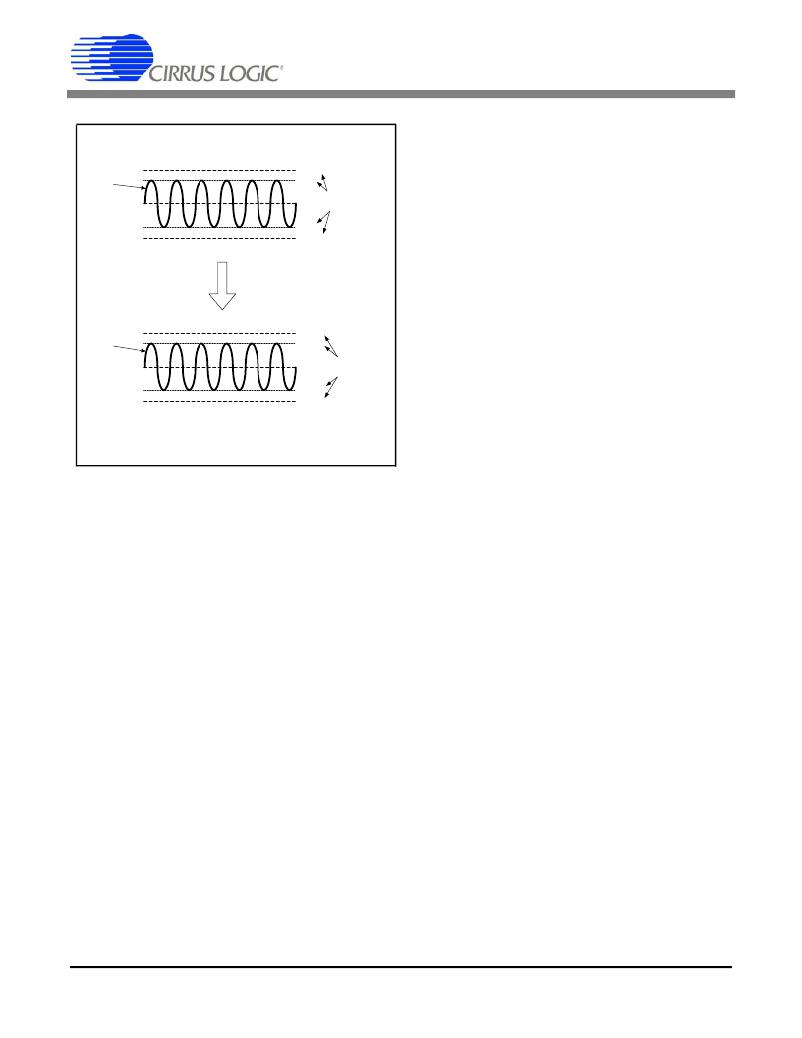
�Before� AC� Gain� Calibration� (Vgain� Register� =� 1)�
�the� DC� voltage� gain� calibration� has� been� executed,�
�250� mV�
�0.9999...�
�the� Instantaneous� Voltage� Register� will� read�
�Sinewave�
�230� mV�
�0.92�
�full-scale� whenever� the� DC� level� of� the� input� signal�
�INPUT�
�SIGNAL�
�0V�
�Instantaneous� Voltage�
�Register� Values�
�is� equal� to� the� level� of� the� DC� calibration� signal� that�
�-230� mV�
�-250� mV�
�V� RMS� Register� =� 230� /� 250� x� 1� /� ?� 2� ??� 0.65054�
�-0.92�
�-1.0000...�
�was� applied� to� the� voltage� channel� inputs� during�
�the� DC� gain� calibration.� For� example,� if� a� +230� mV�
�DC� signal� is� applied� to� the� voltage� channel� inputs�
�during� the� DC� gain� calibration� for� the� current� chan-�
�nel,� then� the� Instantaneous� Voltage� Register� will�
�measure� unity� whenever� a� 230� mV� DC� level� is� ap-�
�After� AC� Gain� Calibration� (Vgain� Register� changed� to� ~0.9223)�
�250� mV� 0.92231�
�plied� to� the� voltage� channel� inputs.�
�Sinewave�
�230� mV�
�0.84853�
�3.8.8� Duration� of� Calibration� Sequence�
�INPUT�
�SIGNAL�
�0V�
�Instantaneous� Voltage�
�Register� Values�
�The� value� of� the� Cycle� Count� Register� (N)� deter-�
�-230� mV�
�-0.84853�
�mines� the� number� of� conversions� that� will� be� per-�
�-250� mV�
�V� RMS� Register� =� ?� 0.6000...�
�-0.92231�
�formed� by� the� CS5460A� during� a� given� calibration�
�sequence.� For� DC� offset/gain� calibrations,� the� cal-�
�Figure� 19.� Example� of� AC� Gain� Calibration�
�3.8.7.2� DC� Offset� Calibration� Sequence�
�The� Voltage� Channel� DC� Offset� Register� holds� the�
�negative� of� the� simple� average� of� N� samples� taken�
�while� the� DC� voltage� offset� calibration� was� execut-�
�ed.� The� inputs� should� be� grounded� during� DC� off-�
�set� calibration.� The� DC� offset� value� is� added� to� the�
�signal� path� to� nullify� the� DC� offset� in� the� system.�
�3.8.7.3� AC� Gain� Calibration� Sequence�
�The� AC� voltage� gain� calibration� algorithm� attempts�
�to� adjust� the� Voltage� Channel� Gain� Register� value�
�such� that� the� calibration� reference� signal� level� pre-�
�sented� at� the� voltage� inputs� will� result� in� a� value� of�
�0.6� in� the� RMS� Voltage� Register.� The� AC� calibra-�
�tion� signal� is� applied� to� the� “+”� and� “-”� input� pins� of�
�the� channel� under� calibration.� During� AC� voltage�
�gain� calibration,� the� value� in� the� RMS� Voltage� Reg-�
�ister� is� divided� into� 0.6.� This� result� is� the� AC� gain�
�calibration� value� stored� in� the� Voltage� Channel�
�Gain� Register.�
�3.8.7.4� DC� Gain� Calibration� Sequence�
�Based� on� the� level� of� the� positive� DC� calibration�
�voltage� that� should� be� applied� across� the� “+”� and�
�“-”� inputs,� the� CS5460A� determines� the� Voltage�
�Channel� Gain� Register� value� by� averaging� the� In-�
�stantaneous� Voltage� Register’s� output� signal� val-�
�DS487F5�
�ibration� sequence� always� takes� at� least� N� +� 30�
�conversion� cycles� to� complete.� For� AC� offset/gain�
�calibrations,� the� calibration� sequence� takes� at�
�least� 6N� +� 30� A/D� conversion� cycles� to� complete,�
�(about� 6� computation� cycles).� If� N� is� increased,� the�
�accuracy� of� calibration� results� will� increase.�
�For� more� information� on� Calibration,� see� AN227� ,�
�“CALIBRATING� THE� CS5460A”.�
�3.9� Phase� Compensation�
�The� values� of� bits� 23� to� 17� in� the� Configuration�
�Register� can� be� altered� to� adjust� the� amount� of�
�time� delay� that� is� imposed� on� the� digitally� sampled�
�voltage� channel� signal.� This� time� delay� is� applied�
�to� the� voltage� channel� signal� in� order� to� compen-�
�sate� for� the� relative� phase� delay� (with� respect� to�
�the� fundamental� frequency)� between� the� sensed�
�voltage� and� current� signals.� Voltage� and� current�
�transformers,� as� well� as� other� sensor/filter/protec-�
�tion� devices� deployed� at� the� front-end� of� the� volt-�
�age/current� sensor� networks� can� often� introduce� a�
�phase-delay� in� the� system� that� distorts/corrupts�
�the� phase� relationship� between� the� line-voltage�
�and� line-current� signals� that� are� to� be� measured.�
�The� phase� compensation� bits� PC[6:0]� in� the� Con-�
�figuration� Register� can� be� set� to� nullify� this� undesir-�
�able� phase� distortion� between� the� digitally�
�sampled� signals� in� the� two� channels.� The� value� in�
�the� 7-bit� phase� compensation� word� indicates� the�
�amount� of� time� delay� that� is� imposed� on� the� volt-�
�31�
�相关PDF资料 |
PDF描述 |
|---|---|
| T95Z156K020ESSL | CAP TANT 15UF 20V 10% 2910 |
| DFN0.83BK | DURA-FLEX .83" BLACK 100' |
| MAX6983AUG+ | IC LED DRIVER LINEAR 24-TSSOP |
| VI-J5H-CX-F4 | CONVERTER MOD DC/DC 52V 75W |
| RSM40DTAD-S189 | CONN EDGECARD 80POS R/A .156 SLD |
相关代理商/技术参数 |
参数描述 |
|---|---|
| CS5460A-BSZ | 制造商:Cirrus Logic 功能描述:Driver IC 制造商:Cirrus Logic 功能描述:IC ENERGY METERING 1PHASE 24SSOP 制造商:Cirrus Logic 功能描述:IC, ENERGY METERING, 1PHASE, 24SSOP |
| CS5460A-BSZR | 功能描述:电流和电力监控器、调节器 IC Sngl-Phs BiDirect PWR/Energy RoHS:否 制造商:STMicroelectronics 产品:Current Regulators 电源电压-最大:48 V 电源电压-最小:5.5 V 工作温度范围:- 40 C to + 150 C 安装风格:SMD/SMT 封装 / 箱体:HPSO-8 封装:Reel |
| CS5460-BS | 制造商:Rochester Electronics LLC 功能描述:- Bulk 制造商:Cirrus Logic 功能描述: |
| CS5460C-ISZ | 功能描述:电流和电力监控器、调节器 Sngl-Phs Bi-Drctnl Power/Energy RoHS:否 制造商:STMicroelectronics 产品:Current Regulators 电源电压-最大:48 V 电源电压-最小:5.5 V 工作温度范围:- 40 C to + 150 C 安装风格:SMD/SMT 封装 / 箱体:HPSO-8 封装:Reel |
| CS5460C-ISZR | 功能描述:电流和电力监控器、调节器 IC Sngl-Phs BiDirect PWR/Energy RoHS:否 制造商:STMicroelectronics 产品:Current Regulators 电源电压-最大:48 V 电源电压-最小:5.5 V 工作温度范围:- 40 C to + 150 C 安装风格:SMD/SMT 封装 / 箱体:HPSO-8 封装:Reel |
发布紧急采购,3分钟左右您将得到回复。