- 您现在的位置:买卖IC网 > PDF目录1992 > CY28548ZXC (Silicon Laboratories Inc)IC CLK CK505 960M/965M 64TSSOP PDF资料下载
参数资料
| 型号: | CY28548ZXC |
| 厂商: | Silicon Laboratories Inc |
| 文件页数: | 23/30页 |
| 文件大小: | 0K |
| 描述: | IC CLK CK505 960M/965M 64TSSOP |
| 标准包装: | 28 |
| 类型: | 时钟/频率发生器 |
| PLL: | 是 |
| 主要目的: | Intel CPU 服务器 |
| 输入: | 时钟 |
| 输出: | LVCMOS |
| 电路数: | 1 |
| 比率 - 输入:输出: | 3:22 |
| 差分 - 输入:输出: | 无/是 |
| 频率 - 最大: | 400MHz |
| 电源电压: | 3.135 V ~ 3.465 V |
| 工作温度: | 0°C ~ 85°C |
| 安装类型: | 表面贴装 |
| 封装/外壳: | 64-TFSOP (0.240",6.10mm 宽) |
| 供应商设备封装: | 64-TSSOP |
| 包装: | 管件 |
第1页第2页第3页第4页第5页第6页第7页第8页第9页第10页第11页第12页第13页第14页第15页第16页第17页第18页第19页第20页第21页第22页当前第23页第24页第25页第26页第27页第28页第29页第30页
CY28548
........................Document #: 001-08400 Rev ** Page 3 of 30
8
PCI0 / CR#_A
I/O, SE 33 MHz Clock/3.3V Clock Request # Input
Mappable via I2C to control either SRC 0 or SRC 2. Default PCI0.
To configure this pin to serve as a Clock Request pin for either SRC pair 2 or pair
0 using the CR#_A_EN bit located in byte 5 bit 7, first disable PCI output (Hi-z) in
byte 2, bit 1.
0 = PCI0 enabled (default)
1= CR#_A enabled.
Byte 5, bit 6 controls whether CR#_A controls SRC0 or SRC2 pair
Byte 5, bit 6:
0 = CR#_A controls SRC0 pair (default)
1= CR#_A controls SRC2 pair
9
VDD_PCI
PWR
3.3V power supply for PCI PLL
10
PCI1 / CR#_B
I/O, SE 33 MHz Clock/3.3V Clock Request # Input
Mappable via I2C to control either SRC 1 or SRC 4. Default PCI1.
To configure this pin to serve as a Clock Request pin for either SRC pair 1 or pair
4 using the CR#_B_EN bit located in byte 5, bit 5, first disable PCI output (Hi-z) in
byte 2, bit 1.
0 = PCI1 enabled (default)
1= CR#_B enabled.
Byte 5, bit 4 controls whether CR#_B controls SRC1 or SRC4 pair
Byte 5, bit 4:
0 = CR#_B controls SRC1 pair (default)
1= CR#_B controls SRC4 pair
11
PCI2 / TME
I/O, SE 33 MHz Clock output/3.3V-tolerance input for enabling Trusted Mode
Sampled at CKPWRGD assertion:
0 = Normal mode, 1 = Trusted mode (no overclocking)
12
PCI3
O, SE 33 MHz Clock output
13
PCI4 / GCLK_SEL
I/O, SE 33 MHz Clock output/3.3V-tolerant input for selecting graphic clock source
on pin 20, 21, 24 and 25
Sampled on CKPWRGD assertion;
14
PCIF0 / ITP_EN
I/O, SE 33 MHz free running clock output/3.3V LVTTL input to enable SRC8 or
CPU2_ITP (sampled on the CKPWRGD assertion)
1 = CPU2_ITP, 0 = SRC8
15
VSS_PCI
GND
Ground for outputs.
16
VDD_48
PWR
3.3V power supply for outputs and PLL.
17
USB_48 / FSA
I/O
Fixed 48 MHz clock output/3.3V-tolerant input for CPU frequency selection
Refer to DC Electrical Specifications table for Vil_FS and Vih_FS specifications.
18
VSS_48
GND
Ground for outputs.
19
VDD_IO
PWR
3.3V-1.25V power supply for outputs
20
SRCT0 / DOT96T
O, DIF True 100 MHz Differential serial reference clocks/Fixed True 96 MHz clock
output. Selected via GCLK_SEL at CKPWRGD assertion
21
SRCC0 / DOT96C
O, DIF Complementary 100 MHz Differential serial reference clocks/Fixed
complement 96 MHz clock output.
Selected via GCLK_SEL at CKPWRGD assertion
22
VSS_IO
GND
Ground for outputs.
23
VDD_PLL3
PWR
3.3V Power supply for PLL3.
24
SRCT1 /
LCDT_100/27M_NSS
O, DIF,
SE
True 100 MHz differential serial reference clock output/True 100 MHz LCD
video clock output / Non spread 27-MHz video clock output.
Selected via GCLK_SEL at CKPWRGD assertion.
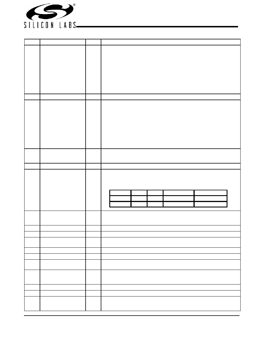
QFN Pin Definitions (continued)
Pin No.
Name
Type
Description
GCLK_SEL
Pin 20
Pin 21
Pin 24
Pin 25
0
DOT96T DOT96C SRC1T/LCD_100T SRC1C/LCD_100C
1
SRCT0
SRCC0
27M_NSS
27M_SS
相关PDF资料 |
PDF描述 |
|---|---|
| CY28551LFXC-3T | IC CLOCK INTEL/AMD SIS VIA 56QFN |
| CY28551LFXC | IC CLOCK INTEL/AMD SIS VIA 64QFN |
| CY2SSTV855ZXI | IC CLOCK DIFFDRV PLL DDR 28TSSOP |
| CY2SSTV857ZXI-27 | IC CLK DDR266/333BUF1:10 48TSSOP |
| CY2SSTV857ZXI-32 | IC CLK DDR266/333BUF1:10 48TSSOP |
相关代理商/技术参数 |
参数描述 |
|---|---|
| CY28548ZXCT | 功能描述:时钟发生器及支持产品 Intel 960/965M Crest line CK505 Intg Vreg RoHS:否 制造商:Silicon Labs 类型:Clock Generators 最大输入频率:14.318 MHz 最大输出频率:166 MHz 输出端数量:16 占空比 - 最大:55 % 工作电源电压:3.3 V 工作电源电流:1 mA 最大工作温度:+ 85 C 安装风格:SMD/SMT 封装 / 箱体:QFN-56 |
| CY28551 | 制造商:CYPRESS 制造商全称:Cypress Semiconductor 功能描述:Universal Clock Generator for Intel, VIA, and SIS㈢ |
| CY28551-3 | 制造商:CYPRESS 制造商全称:Cypress Semiconductor 功能描述:Universal Clock Generator for Intel, VIA and SIS㈢ |
| CY28551LFXC | 功能描述:时钟发生器及支持产品 Universal System Clk Intel AMD SiS Via RoHS:否 制造商:Silicon Labs 类型:Clock Generators 最大输入频率:14.318 MHz 最大输出频率:166 MHz 输出端数量:16 占空比 - 最大:55 % 工作电源电压:3.3 V 工作电源电流:1 mA 最大工作温度:+ 85 C 安装风格:SMD/SMT 封装 / 箱体:QFN-56 |
| CY28551LFXC-3 | 功能描述:时钟发生器及支持产品 Universal System Clk Intel AMD SiS Via RoHS:否 制造商:Silicon Labs 类型:Clock Generators 最大输入频率:14.318 MHz 最大输出频率:166 MHz 输出端数量:16 占空比 - 最大:55 % 工作电源电压:3.3 V 工作电源电流:1 mA 最大工作温度:+ 85 C 安装风格:SMD/SMT 封装 / 箱体:QFN-56 |
发布紧急采购,3分钟左右您将得到回复。