- 您现在的位置:买卖IC网 > PDF目录1992 > CY28548ZXC (Silicon Laboratories Inc)IC CLK CK505 960M/965M 64TSSOP PDF资料下载
参数资料
| 型号: | CY28548ZXC |
| 厂商: | Silicon Laboratories Inc |
| 文件页数: | 29/30页 |
| 文件大小: | 0K |
| 描述: | IC CLK CK505 960M/965M 64TSSOP |
| 标准包装: | 28 |
| 类型: | 时钟/频率发生器 |
| PLL: | 是 |
| 主要目的: | Intel CPU 服务器 |
| 输入: | 时钟 |
| 输出: | LVCMOS |
| 电路数: | 1 |
| 比率 - 输入:输出: | 3:22 |
| 差分 - 输入:输出: | 无/是 |
| 频率 - 最大: | 400MHz |
| 电源电压: | 3.135 V ~ 3.465 V |
| 工作温度: | 0°C ~ 85°C |
| 安装类型: | 表面贴装 |
| 封装/外壳: | 64-TFSOP (0.240",6.10mm 宽) |
| 供应商设备封装: | 64-TSSOP |
| 包装: | 管件 |
第1页第2页第3页第4页第5页第6页第7页第8页第9页第10页第11页第12页第13页第14页第15页第16页第17页第18页第19页第20页第21页第22页第23页第24页第25页第26页第27页第28页当前第29页第30页
CY28548
........................Document #: 001-08400 Rev ** Page 8 of 30
Frequency Select Pin (FSA, FSB and FSC)
Apply the appropriate logic levels to FSA, FSB, and FSC
inputs before CK-PWRGD assertion to achieve host clock
frequency selection. When the clock chip sampled HIGH on
CK-PWRGD and indicates that VTT voltage is stable then
FSA, FSB, and FSC input values are sampled. This process
employs a one-shot functionality and once the CK-PWRGD
sampled a valid HIGH, all other FSA, FSB, FSC, and
CK-PWRGD transitions are ignored except in test mode
Serial Data Interface
To enhance the flexibility and function of the clock synthesizer,
a two-signal serial interface is provided. Through the Serial
Data Interface, various device functions, such as individual
clock output buffers are individually enabled or disabled. The
registers associated with the Serial Data Interface initialize to
their default setting at power-up. The use of this interface is
optional. Clock device register changes are normally made at
system initialization, if any are required. The interface cannot
be used during system operation for power management
functions.
Data Protocol
The clock driver serial protocol accepts byte write, byte read,
block write, and block read operations from the controller. For
block write/read operation, Access the bytes in sequential
order from lowest to highest (most significant bit first) with the
ability to stop after any complete byte is transferred. For byte
write and byte read operations, the system controller can
access individually indexed bytes. The offset of the indexed
byte is encoded in the command code described in Table 2.
The block write and block read protocol is outlined in Table 3
while Table 4 outlines byte write and byte read protocol. The
slave receiver address is 11010010 (D2h)
.
57
FSB / TEST_MODE
I
3.3V-tolerant input for CPU frequency selection / Selects Ref/N or Tri-state
when in test mode:
0 = Tri-state, 1 = Ref/N
Refer to DC Electrical Specifications table for Vil_FS and Vih_FS specifications.
58
VSS_REF
GND
Ground for outputs.
59
Xout
O, SE 14.318 MHz Crystal output.
60
Xin
I
14.318 MHz Crystal input.
61
VDD_REF
PWR
3.3V Power supply for outputs and also maintains SMBUS registers during
power down.
62
REF0 / FSC / TEST_SEL
I/O
Fixed 14.318 clock output / 3.3V-tolerant input for CPU frequency selection /
Selects test mode if pulled to VIHFS_C when CK_PWRGD is asserted HIGH.
Refer to DC Electrical Specifications table for VILFS_C, VIMFS_C, VIHFS_C specifica-
tions.
63
SDATA
I/O
SMBus-compatible SDATA.
64
SCLK
I
SMBus-compatible SCLOCK.
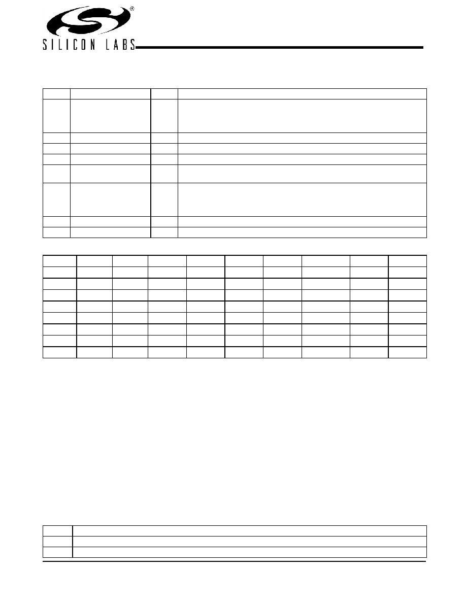
TSSOP Pin Definitions (continued)
Pin No.
Name
Type
Description
Table 1. Frequency Select Pin (FSA, FSB and FSC)
FSC
FSB
FSA
CPU
SRC
PCIF/PCI
27MHz
REF
DOT96
USB
0
266 MHz
100 MHz
33 MHz
27 MHz
14.318 MHz
96 MHz
48 MHz
0
1
133 MHz
100 MHz
33 MHz
27 MHz
14.318 MHz
96 MHz
48 MHz
0
1
0
200 MHz
100 MHz
33 MHz
27 MHz
14.318 MHz
96 MHz
48 MHz
0
1
166 MHz
100 MHz
33 MHz
27 MHz
14.318 MHz
96 MHz
48 MHz
1
0
333 MHz
100 MHz
33 MHz
27 MHz
14.318 MHz
96 MHz
48 MHz
1
0
1
100 MHz
33 MHz
27 MHz
14.318 MHz
96 MHz
48 MHz
1
0
400 MHz
100 MHz
33 MHz
27 MHz
14.318 MHz
96 MHz
48 MHz
1
Reserved
Table 2. Command Code Definition
Bit
Description
7
0 = Block read or block write operation, 1 = Byte read or byte write operation
(6:0)
Byte offset for byte read or byte write operation. For block read or block write operations, these bits should be '0000000'
相关PDF资料 |
PDF描述 |
|---|---|
| CY28551LFXC-3T | IC CLOCK INTEL/AMD SIS VIA 56QFN |
| CY28551LFXC | IC CLOCK INTEL/AMD SIS VIA 64QFN |
| CY2SSTV855ZXI | IC CLOCK DIFFDRV PLL DDR 28TSSOP |
| CY2SSTV857ZXI-27 | IC CLK DDR266/333BUF1:10 48TSSOP |
| CY2SSTV857ZXI-32 | IC CLK DDR266/333BUF1:10 48TSSOP |
相关代理商/技术参数 |
参数描述 |
|---|---|
| CY28548ZXCT | 功能描述:时钟发生器及支持产品 Intel 960/965M Crest line CK505 Intg Vreg RoHS:否 制造商:Silicon Labs 类型:Clock Generators 最大输入频率:14.318 MHz 最大输出频率:166 MHz 输出端数量:16 占空比 - 最大:55 % 工作电源电压:3.3 V 工作电源电流:1 mA 最大工作温度:+ 85 C 安装风格:SMD/SMT 封装 / 箱体:QFN-56 |
| CY28551 | 制造商:CYPRESS 制造商全称:Cypress Semiconductor 功能描述:Universal Clock Generator for Intel, VIA, and SIS㈢ |
| CY28551-3 | 制造商:CYPRESS 制造商全称:Cypress Semiconductor 功能描述:Universal Clock Generator for Intel, VIA and SIS㈢ |
| CY28551LFXC | 功能描述:时钟发生器及支持产品 Universal System Clk Intel AMD SiS Via RoHS:否 制造商:Silicon Labs 类型:Clock Generators 最大输入频率:14.318 MHz 最大输出频率:166 MHz 输出端数量:16 占空比 - 最大:55 % 工作电源电压:3.3 V 工作电源电流:1 mA 最大工作温度:+ 85 C 安装风格:SMD/SMT 封装 / 箱体:QFN-56 |
| CY28551LFXC-3 | 功能描述:时钟发生器及支持产品 Universal System Clk Intel AMD SiS Via RoHS:否 制造商:Silicon Labs 类型:Clock Generators 最大输入频率:14.318 MHz 最大输出频率:166 MHz 输出端数量:16 占空比 - 最大:55 % 工作电源电压:3.3 V 工作电源电流:1 mA 最大工作温度:+ 85 C 安装风格:SMD/SMT 封装 / 箱体:QFN-56 |
发布紧急采购,3分钟左右您将得到回复。