- 您现在的位置:买卖IC网 > PDF目录256924 > CY38015V144-66BBC (CYPRESS SEMICONDUCTOR CORP) LOADABLE PLD, 18.9 ns, PBGA144 PDF资料下载
参数资料
| 型号: | CY38015V144-66BBC |
| 厂商: | CYPRESS SEMICONDUCTOR CORP |
| 元件分类: | PLD |
| 英文描述: | LOADABLE PLD, 18.9 ns, PBGA144 |
| 封装: | FBGA-144 |
| 文件页数: | 5/32页 |
| 文件大小: | 929K |
| 代理商: | CY38015V144-66BBC |
第1页第2页第3页第4页当前第5页第6页第7页第8页第9页第10页第11页第12页第13页第14页第15页第16页第17页第18页第19页第20页第21页第22页第23页第24页第25页第26页第27页第28页第29页第30页第31页第32页
PRELIMINARY
Quantum38K ISR
CPLD Family
Document #: 38-03043 Rev. **
Page 13 of 32
Power-up Sequence Requirements
Upon power-up, all the outputs remain three-stated until all
the VCC pins have powered-up to the nominal voltage and
the part has completed configuration.
The part will not start configuration until VCC, VCCIO,
VCCJTAG, and VCCCNFG have reached nominal voltage.
VCC pins can be powered up in any order. This includes
VCC, VCCIO, VCCJTAG, and VCCCNFG.
All VCCIOs on a bank should be tied to the same potential
and powered up together.
All VCCIOs (even the unused banks) need to be powered up
to at least 1.5V before configuration has completed.
Maximum ramp time for all VCCs should be 0V to nominal
voltage in 100 ms.
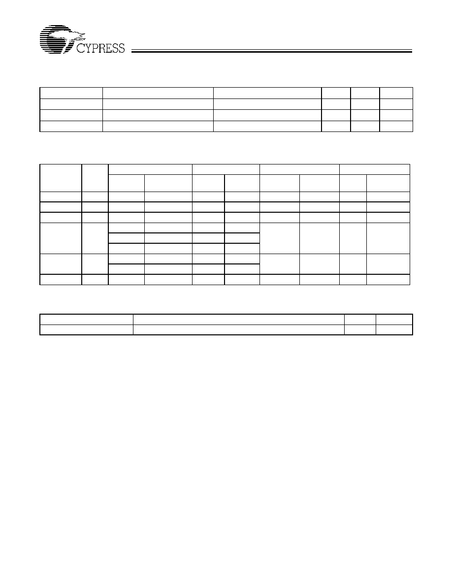
Capacitance
Parameter
Description
Test Conditions
Min.
Max.
Unit
CI/O
Input/Output Capacitance
Vin=VCCIO @ f=1MHz 25°C
10
pF
CCLK
Clock Signal Capacitance
Vin=VCCIO @ f=1MHz 25°C
5
12
pF
CPCI
PCI Compliant[5] Capacitance
Vin=VCCIO @ f=1MHz 25°C
8
pF
DC Characteristics[6] (IO)
Input/
Output
Standard
VCCIO
(V)
VOH (V)
VOL (V)
VIH (V)
VIL (V)
@ IOH =VOH (min.)
@ IOL =
VOL
(max.)
Min.
Max.
Min.
Max.
LVTTL
3.3
–4 mA
2.4
4 mA
0.4
2.0 V
VCCIO+0.3
–0.3V
0.8V
LVCMOS
3.3
–0.1 mA
VCCIO–0.2v
0.1 mA
0.2
2.0 V
VCCIO+0.3
–0.3V
0.8V
LVCMOS3
3.0
–0.1 mA
VCCIO–0.2v
0.1mA
0.2
2.0 V
VCCIO+0.3
–0.3V
0.8V
LVCMOS2
2.5
–0.1 mA
2.1
0.1 mA
0.2
1.7 V
VCCIO+0.3
–0.3V
0.7V
–1.0 mA
2.0
1.0 mA
0.4
–2.0 mA
1.7
2.0 mA
0.7
LVCMOS18
1.8
–0.1 mA
VCCIO–0.2v
0.1 mA
0.2
0.65VCCIO
VCCIO+0.3
–0.3V
0.35VCCIO
–2 mA
VCCIO–0.45v
2.0 mA
0.45
3.3V PCI
3.3
–0.5 mA
0.9VCCIO
1.5 mA
0.1VCCIO
0.5VCCIO
VCCIO+0.5
–0.5V
0.3VCCIO
Configuration Parameters
Parameter
Description
Min.
Unit
tRECONFIG
Reconfig pin LOW time before it goes HIGH
200
ns
Note:
5.
PCI spec (rev 2.2) requires the IDSEL pin to have capacitance less than or equal to 8 pF. Document titled “Quantum38K Pin Tables” identifies all the I/O pins,
in a given package, which can be used as IDSEL in a PCI design. All other I/O pins meet the PCI requirement of capacitance less than or equal to 10pF.
6.
The number of I/Os which can be used in each I/O bank depends on the type of I/O standards and the number of VCCIO and GND pins being used. Please
refer to the application note titled “Delta39K and Quantum38K Device I/O Standards and Configurations” for details.
The source current limit per I/O bank per Vccio pin is 165 mA
The sink current limit per I/O bank per GND pin is 230 mA
相关PDF资料 |
PDF描述 |
|---|---|
| CY38015V144-66BBI | LOADABLE PLD, 18.9 ns, PBGA144 |
| CY38015V144-83BBC | LOADABLE PLD, 15 ns, PBGA144 |
| CY38015V144-83BBI | LOADABLE PLD, 15 ns, PBGA144 |
| CY38015V208-66NC | LOADABLE PLD, 18.9 ns, PQFP208 |
| CY38015V208-66NI | LOADABLE PLD, 18.9 ns, PQFP208 |
相关代理商/技术参数 |
参数描述 |
|---|---|
| CY38050V208-125NTC | 制造商:Cypress Semiconductor 功能描述:CPLD QUANTUM38K 72K GATES 768 MCRCLLS COMM 0.18UM 2.5V/3.3V - Bulk |
| CY38050V208-125NTI | 制造商:Cypress Semiconductor 功能描述:CPLD QUANTUM38K 72K GATES 768 MCRCLLS IND 0.18UM 2.5V/3.3V 2 - Bulk |
| CY38050V208-83NTC | 制造商:Cypress Semiconductor 功能描述:CPLD QUANTUM38K 72K GATES 768 MCRCLLS COMM 0.18UM 2.5V/3.3V - Bulk |
| CY38050V208-83NTI | 制造商:Cypress Semiconductor 功能描述:CPLD QUANTUM38K 72K GATES 768 MCRCLLS IND 0.18UM 2.5V/3.3V 2 - Bulk |
| CY38100V208-125NTI | 制造商:Cypress Semiconductor 功能描述:CPLD QUANTUM38K 144K GATES 1536 MCRCLLS IND 0.18UM 2.5V/3.3V - Bulk |
发布紧急采购,3分钟左右您将得到回复。