- 您现在的位置:买卖IC网 > PDF目录295374 > CY7C1387DV25-225BZI (CYPRESS SEMICONDUCTOR CORP) 1M X 18 CACHE SRAM, 2.8 ns, PBGA165 PDF资料下载
参数资料
| 型号: | CY7C1387DV25-225BZI |
| 厂商: | CYPRESS SEMICONDUCTOR CORP |
| 元件分类: | SRAM |
| 英文描述: | 1M X 18 CACHE SRAM, 2.8 ns, PBGA165 |
| 封装: | 13 X 15 MM, 1.40 MM HEIGHT, FBGA-165 |
| 文件页数: | 29/32页 |
| 文件大小: | 501K |
| 代理商: | CY7C1387DV25-225BZI |
第1页第2页第3页第4页第5页第6页第7页第8页第9页第10页第11页第12页第13页第14页第15页第16页第17页第18页第19页第20页第21页第22页第23页第24页第25页第26页第27页第28页当前第29页第30页第31页第32页
PRELIMINARY
CY7C1386DV25
CY7C1387DV25
Document #: 38-05548 Rev. **
Page 6 of 32
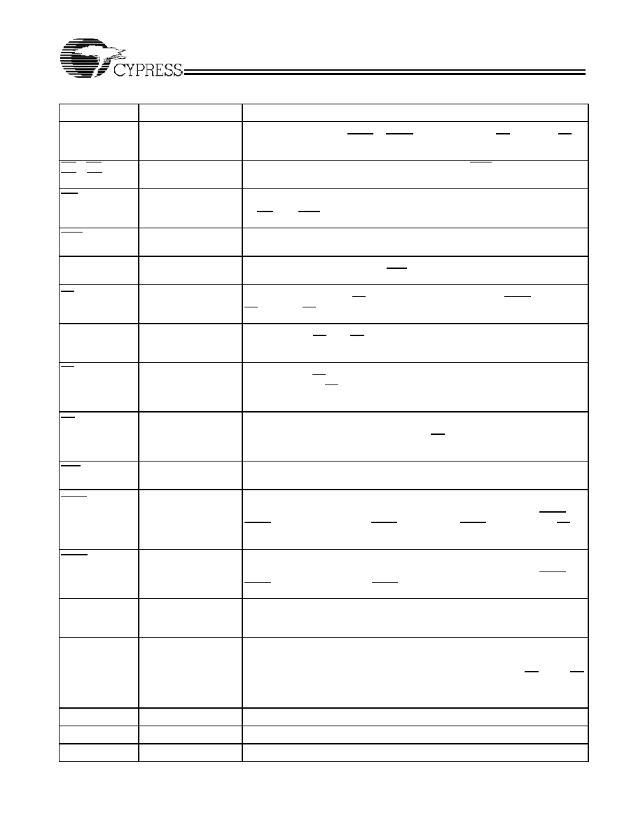
Pin Definitions
Name
I/O
Description
A0, A1, A
Input-
Synchronous
Address Inputs used to select one of the address locations. Sampled at the
rising edge of the CLK if ADSP or ADSC is active LOW, and CE1, CE2, and CE3[2]
are sampled active. A1: A0 are fed to the two-bit counter..
BWA, BWB
BWC, BWD
Input-
Synchronous
Byte Write Select Inputs, active LOW. Qualified with BWE to conduct byte writes
to the SRAM. Sampled on the rising edge of CLK.
GW
Input-
Synchronous
Global Write Enable Input, active LOW. When asserted LOW on the rising edge
of CLK, a global write is conducted (ALL bytes are written, regardless of the values
on BWX and BWE).
BWE
Input-
Synchronous
Byte Write Enable Input, active LOW. Sampled on the rising edge of CLK. This
signal must be asserted LOW to conduct a byte write.
CLK
Input-
Clock
Clock Input. Used to capture all synchronous inputs to the device. Also used to
increment the burst counter when ADV is asserted LOW, during a burst operation.
CE1
Input-
Synchronous
Chip Enable 1 Input, active LOW. Sampled on the rising edge of CLK. Used in
conjunction with CE2 and CE3[2] to select/deselect the device. ADSP is ignored if
CE1 is HIGH. CE1 is sampled only when a new external address is loaded.
CE2[2]
Input-
Synchronous
Chip Enable 2 Input, active HIGH. Sampled on the rising edge of CLK. Used in
conjunction with CE1 and CE3[2] to select/deselect the device. CE2 is sampled only
when a new external address is loaded.
CE3[2]
Input-
Synchronous
Chip Enable 3 Input, active LOW. Sampled on the rising edge of CLK. Used in
conjunction with CE1 and CE2 to select/deselect the device. Not connected for BGA.
Where referenced, CE3[2] is assumed active throughout this document for BGA.
CE3 is sampled only when a new external address is loaded.
OE
Input-
Asynchronous
Output Enable, asynchronous input, active LOW. Controls the direction of the
I/O pins. When LOW, the I/O pins behave as outputs. When deasserted HIGH, DQ
pins are tri-stated, and act as input data pins. OE is masked during the first clock of
a read cycle when emerging from a deselected state.
ADV
Input-
Synchronous
Advance Input signal, sampled on the rising edge of CLK, active LOW. When
asserted, it automatically increments the address in a burst cycle.
ADSP
Input-
Synchronous
Address Strobe from Processor, sampled on the rising edge of CLK, active
LOW. When asserted LOW, addresses presented to the device are captured in the
address registers. A1: A0 are also loaded into the burst counter. When ADSP and
ADSC are both asserted, only ADSP is recognized. ASDP is ignored when CE1 is
deasserted HIGH.
ADSC
Input-
Synchronous
Address Strobe from Controller, sampled on the rising edge of CLK, active
LOW. When asserted LOW, addresses presented to the device are captured in the
address registers. A1: A0 are also loaded into the burst counter. When ADSP and
ADSC are both asserted, only ADSP is recognized.
ZZ
Input-
Asynchronous
ZZ “sleep” Input, active HIGH. When asserted HIGH places the device in a
non-time-critical “sleep” condition with data integrity preserved. For normal
operation, this pin has to be LOW or left floating. ZZ pin has an internal pull-down.
DQs, DQPs
I/O-
Synchronous
Bidirectional Data I/O lines. As inputs, they feed into an on-chip data register that
is triggered by the rising edge of CLK. As outputs, they deliver the data contained
in the memory location specified by the addresses presented during the previous
clock rise of the read cycle. The direction of the pins is controlled by OE. When OE
is asserted LOW, the pins behave as outputs. When HIGH, DQs and DQPX are
placed in a tri-state condition.
VDD
Power Supply
Power supply inputs to the core of the device.
VSS
Ground
Ground for the core of the device.
VSSQ
I/O Ground
Ground for the I/O circuitry.
相关PDF资料 |
PDF描述 |
|---|---|
| CY7C1387DV25-225BZC | 1M X 18 CACHE SRAM, 2.8 ns, PBGA165 |
| CY7C138AV | Memory |
| CY7C025-15JC | x16 Dual-Port SRAM |
| CY7C0251AV-20AC | x18 Dual-Port SRAM |
| CY7C0251AV-25AC | x18 Dual-Port SRAM |
相关代理商/技术参数 |
参数描述 |
|---|---|
| CY7C138XC | 制造商:Cypress Semiconductor 功能描述: |
| CY7C139-25JC | 制造商:Cypress Semiconductor 功能描述: |
| CY7C139-25JXC | 功能描述:IC SRAM 36KBIT 25NS 68PLCC RoHS:是 类别:集成电路 (IC) >> 存储器 系列:- 标准包装:1,000 系列:- 格式 - 存储器:RAM 存储器类型:移动 SDRAM 存储容量:256M(8Mx32) 速度:133MHz 接口:并联 电源电压:1.7 V ~ 1.95 V 工作温度:-40°C ~ 85°C 封装/外壳:90-VFBGA 供应商设备封装:90-VFBGA(8x13) 包装:带卷 (TR) 其它名称:557-1327-2 |
| CY7C1392CV18-200BZC | 功能描述:静态随机存取存储器 2Mx8 1.8V DDR II SIO 静态随机存取存储器 RoHS:否 制造商:Cypress Semiconductor 存储容量:16 Mbit 组织:1 M x 16 访问时间:55 ns 电源电压-最大:3.6 V 电源电压-最小:2.2 V 最大工作电流:22 uA 最大工作温度:+ 85 C 最小工作温度:- 40 C 安装风格:SMD/SMT 封装 / 箱体:TSOP-48 封装:Tray |
| CY7C1392CV18-250BZC | 功能描述:静态随机存取存储器 2Mx8 1.8V DDR II SIO 静态随机存取存储器 RoHS:否 制造商:Cypress Semiconductor 存储容量:16 Mbit 组织:1 M x 16 访问时间:55 ns 电源电压-最大:3.6 V 电源电压-最小:2.2 V 最大工作电流:22 uA 最大工作温度:+ 85 C 最小工作温度:- 40 C 安装风格:SMD/SMT 封装 / 箱体:TSOP-48 封装:Tray |
发布紧急采购,3分钟左右您将得到回复。