- 您现在的位置:买卖IC网 > PDF目录20392 > DC1472A (Linear Technology)BOARD DEMO LTM4618 PDF资料下载
参数资料
| 型号: | DC1472A |
| 厂商: | Linear Technology |
| 文件页数: | 19/24页 |
| 文件大小: | 0K |
| 描述: | BOARD DEMO LTM4618 |
| 软件下载: | LTM4618 Spice Model |
| 设计资源: | DC1472A Design Files DC1472A Schematic |
| 标准包装: | 1 |
| 系列: | µModule® |
| 主要目的: | DC/DC,步降 |
| 输出及类型: | 1,非隔离 |
| 输出电压: | 1.2V,1.5V,1.8V,2.5V,3.3V,5V |
| 电流 - 输出: | 6A |
| 输入电压: | 4.5 ~ 26.5 V |
| 稳压器拓扑结构: | 降压 |
| 频率 - 开关: | 500kHz |
| 板类型: | 完全填充 |
| 已供物品: | 板 |
| 已用 IC / 零件: | LTM4618 |
| 相关产品: | LTM4618IV#PBF-ND - IC DC-DC UMODULE BUCK 6A 84-LGA LTM4618EV#PBF-ND - IC DC-DC UMODULE BUCK 6A 84-LGA |
| 其它名称: | DC1472 DC1472-ND |
�� �
�
�LTM4618�
�APPLICATIONS� INFORMATION�
�EMI� Section�
�The� LTM4618� has� been� evaluated� for� CISPR22� A� and� B�
�Radiated� EMI� and� CISPR25� Conducted� EMI.� The� CISPR25�
�Conducted� EMI� test� was� performed� with� an� input� π� ?lter�
�as� shown� in� Figure� 17.� An� RC� snubber� circuit� is� optionally�
�used� from� the� SW� pin� to� the� PGND� pin� to� improve� the� higher�
�frequency� attenuation� and� EMI� limit� guard� band.� Figure� 18�
�shows� the� CISPR25� conducted� emissions� plot� for� 26.5V�
�input� to� 3.3V� output� at� 5A� load.� Several� conditions� were�
�evaluated,� and� Figure� 18� results� are� from� the� worst-case�
�condition.� The� input� π� ?lter� is� used� to� attenuate� the� re?ected�
�noise� from� the� regulator� input,� and� is� primarily� utilized�
�when� the� power� regulators� are� closed� to� the� input� power�
�feed� to� a� board,� like� the� input� power� connectors.� If� the�
�regulator� design� is� placed� out� on� the� center� of� the� system�
�board,� then� the� input� π� ?lter� may� not� be� needed� because�
�all� of� the� extra� board� capacitance� and� the� inductive� planes�
�will� provide� ?ltering� for� re?ected� emissions.� If� the� system�
�board� has� noise� sensitive� circuitry� that� is� powered� from�
�the� same� voltage� rail� as� the� regulators� are,� then� an� input�
�π� ?lter� is� a� good� idea� to� keep� regulator� noise� from� cor-�
�rupting� the� noise� sensitive� circuitry� on� the� system� board.�
�Figure� 19� shows� the� CISPR22� B� Radiated� EMI� plots.� The�
�input� π� ?lter� is� used� to� attenuate� the� re?ected� noise� from�
�?� Use� large� PCB� copper� areas� for� high� current� path,�
�including� V� IN� ,� PGND� and� V� OUT� .� It� helps� to� minimize�
�the� PCB� conduction� loss� and� thermal� stress.�
�?� Test� points� can� be� placed� on� signal� pin� for� monitor-�
�ing� during� testing.�
�?� Place� high� frequency� ceramic� input� and� output�
�capacitors� next� to� the� V� IN� ,� PGND� and� V� OUT� pins� to�
�minimize� high� frequency� noise.�
�?� Place� a� dedicated� power� ground� layer� underneath� the�
�unit.�
�?� To� minimize� the� via� conduction� loss� and� reduce� mod-�
�ule� thermal� stress,� use� multiple� vias� for� interconnec-�
�tion� between� top� layer� and� other� power� layers.�
�?� Do� not� put� vias� directly� on� the� pad,� unless� they� are�
�capped.�
�?� Use� a� separated� SGND� ground� copper� area� for� com-�
�ponents� connected� to� signal� pins.� Connect� the� SGND�
�to� PGND� underneath� the� unit.�
�Figure� 20� gives� a� good� example� of� the� recommended�
�layout.�
�propagating� out� onto� the� input� power� cables,� thus� pos-�
�sibly� causing� radiated� EMI� issues.� An� RC� snubber� circuit�
�is� optionally� used� from� the� SW� pin� to� the� PGND� pin� to�
�improve� the� higher� frequency� attenuation� and� EMI� limit�
�guard� band.� A� placeholder� can� accommodate� the� R� SNUB�
�and� C� SNUB� components� with� 1.2Ω� and� 470pF.� These�
�components� are� probably� not� necessary,� but� can� be� used�
�V� IN�
�7�
�6�
�5�
�PGND�
�or� adjusted� to� improve� the� radiated� limit� guard� bands� at�
�the� higher� frequencies� by� attenuating� any� switch� node�
�ringing� due� to� parasitic� values� in� the� high� speed� switching�
�paths.� It� is� important� to� follow� the� recommended� layout�
�guidelines� and� use� good� X5R� or� X7R� ceramic� capacitors�
�CNTRL�
�4�
�3�
�2�
�1�
�to� get� good� results.�
�A�
�B�
�C�
�D�
�E�
�F�
�G�
�H�
�J�
�K�
�L�
�M�
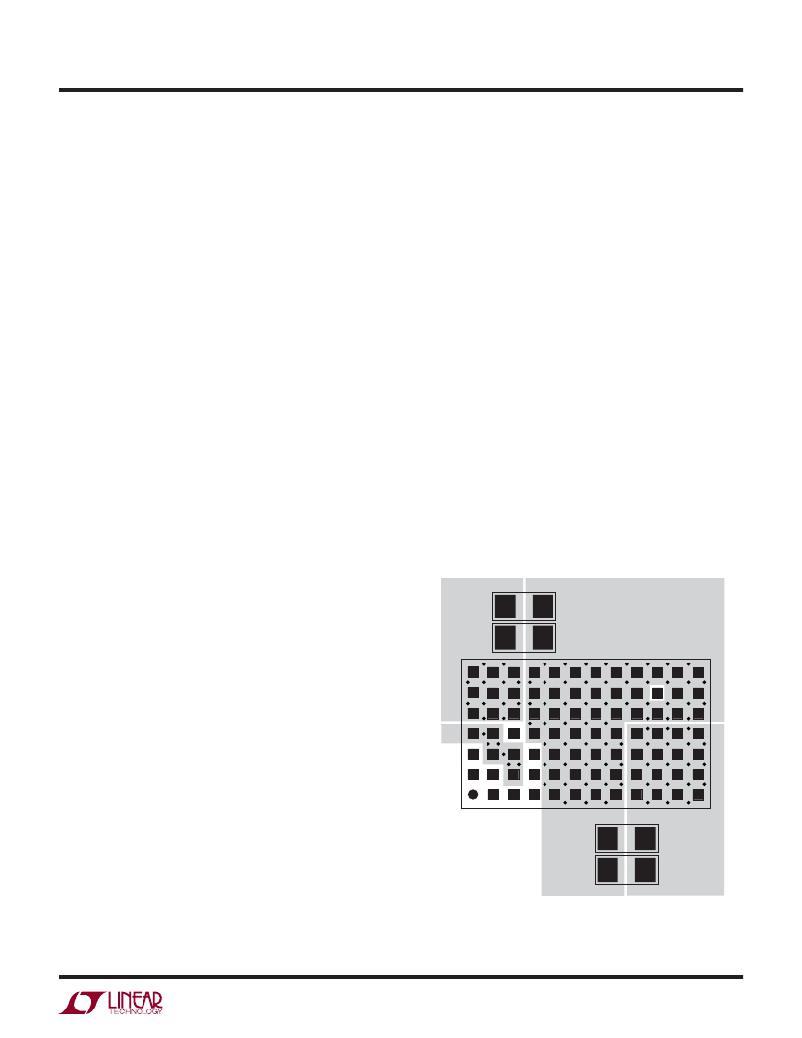
�Layout� Checklist/Example�
�CNTRL�
�C� OUT�
�The� high� integration� of� LTM4618� makes� the� PC� board� layout�
�very� simple� and� easy.� However,� to� optimize� its� electrical�
�PGND�
�C� OUT�
�V� OUT�
�4618� F20�
�and� thermal� performance,� some� layout� considerations�
�are� still� necessary.�
�Figure� 20.� Recommended� PCB� Layout� Example�
�4618fa�
�19�
�相关PDF资料 |
PDF描述 |
|---|---|
| EBM15DTKS | CONN EDGECARD 30POS DIP .156 SLD |
| IR2136S | IC DRIVER BRIDGE 3-PHASE 28-SOIC |
| EL7156CS-T7 | IC PIN DRIVER 40MHZ 3ST 8-SOIC |
| 395-062-521-204 | CARD EDGE 62POS DL .100X.200 BLK |
| F750G108MDC | CAP TANT 1000UF 4V 20% 2917 |
相关代理商/技术参数 |
参数描述 |
|---|---|
| DC1477A | 功能描述:BOARD EVAL LTM4609 RoHS:否 类别:编程器,开发系统 >> 评估板 - DC/DC 与 AC/DC(离线)SMPS 系列:µModule® 标准包装:1 系列:- 主要目的:DC/DC,步降 输出及类型:1,非隔离 功率 - 输出:- 输出电压:3.3V 电流 - 输出:3A 输入电压:4.5 V ~ 28 V 稳压器拓扑结构:降压 频率 - 开关:250kHz 板类型:完全填充 已供物品:板 已用 IC / 零件:L7981 其它名称:497-12113STEVAL-ISA094V1-ND |
| DC1477B | 功能描述:BOARD EVAL LTM4609 RoHS:否 类别:编程器,开发系统 >> 评估板 - DC/DC 与 AC/DC(离线)SMPS 系列:µModule® 标准包装:1 系列:- 主要目的:DC/DC,步降 输出及类型:1,非隔离 功率 - 输出:- 输出电压:3.3V 电流 - 输出:3A 输入电压:4.5 V ~ 28 V 稳压器拓扑结构:降压 频率 - 开关:250kHz 板类型:完全填充 已供物品:板 已用 IC / 零件:L7981 其它名称:497-12113STEVAL-ISA094V1-ND |
| DC1483A | 制造商:Linear Technology 功能描述:EVAL BOARD, LTC3535 100mA SYNC STEP-UP R 制造商:Linear Technology 功能描述:EVAL BOARD, LTC3535 100mA SYNC STEP-UP REG; Silicon Manufacturer:Linear Technology; Silicon Core Number:LTC3535; Kit Application Type:Power Management; Kit Contents:Evaluation Board for LTC3535; Length:42mm |
| DC1485A | 功能描述:BOARD DAC LTC2757 RoHS:是 类别:编程器,开发系统 >> 评估板 - 数模转换器 (DAC) 系列:QuikEval™, SoftSpan™ 产品培训模块:Lead (SnPb) Finish for COTS Obsolescence Mitigation Program 标准包装:1 系列:- DAC 的数量:4 位数:12 采样率(每秒):- 数据接口:串行,SPI? 设置时间:3µs DAC 型:电流/电压 工作温度:-40°C ~ 85°C 已供物品:板 已用 IC / 零件:MAX5581 |
| DC1488A-A | 功能描述:BOARD DAC LTC2634-12 RoHS:是 类别:编程器,开发系统 >> 评估板 - 数模转换器 (DAC) 系列:QuikEval™ 产品培训模块:Lead (SnPb) Finish for COTS Obsolescence Mitigation Program 标准包装:1 系列:- DAC 的数量:4 位数:12 采样率(每秒):- 数据接口:串行,SPI? 设置时间:3µs DAC 型:电流/电压 工作温度:-40°C ~ 85°C 已供物品:板 已用 IC / 零件:MAX5581 |
发布紧急采购,3分钟左右您将得到回复。